Image acquisition module
An image acquisition and image sensing technology, which is applied to image communication, TV, color TV parts, etc., can solve the problems that the image quality cannot be effectively improved, and the image sensor assembly has a large inclination angle, so as to ensure the flatness and reduce the The effect of assembling inclination and improving bonding strength
- Summary
- Abstract
- Description
- Claims
- Application Information
AI Technical Summary
Problems solved by technology
Method used
Image
Examples
no. 1 example 〕
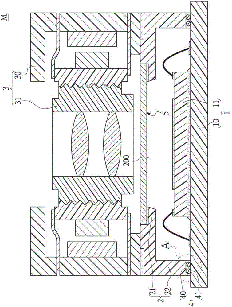
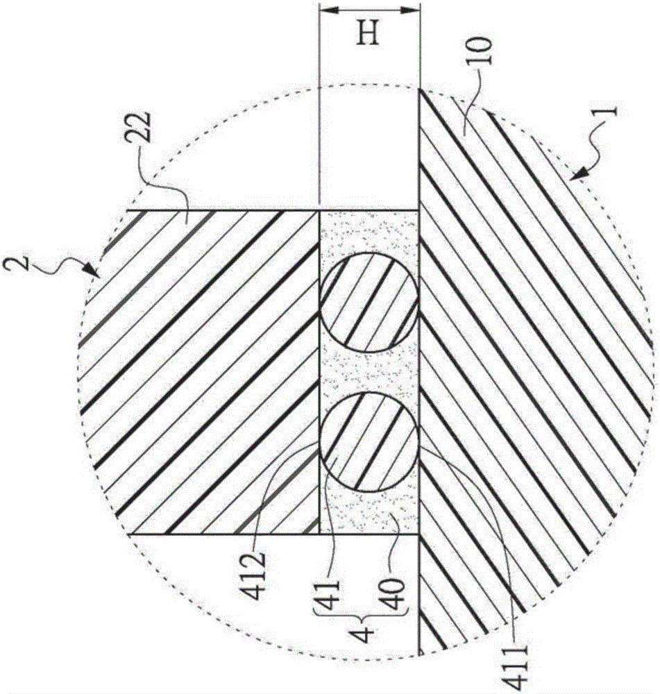
[0037] see figure 1 and figure 2 shown, where figure 2 for figure 1 An enlarged schematic of part A. As can be seen from the above figures, the first embodiment of the present invention provides an image acquisition module M for increasing bonding strength and flatness, which includes: an image sensing unit 1, a frame housing 2 and an actuator structure 3 (optical auxiliary structure).
[0038] First, if figure 1 As shown, the image sensing unit 1 includes a carrier substrate 10 and an image sensing chip 11 disposed on the carrier substrate 10 and electrically connected to the carrier substrate 10 . For example, the image sensing chip 11 can be a CMOS image sensing chip, and the image sensing chip 11 can be provided with an adhesive (not numbered, such as UV adhesive, thermosetting adhesive, or furnace curing adhesive, etc.) on the carrier substrate 10 . In addition, the carrier substrate 10 can be a circuit substrate with a plurality of conductive pads (not labeled) ...
no. 2 example
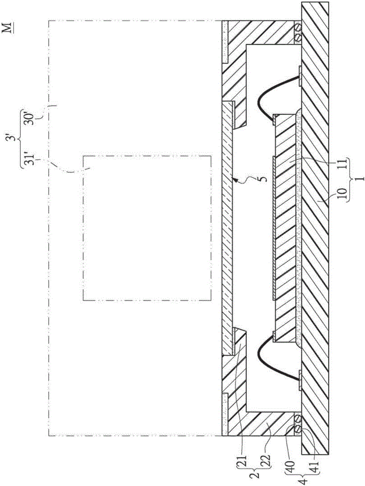
[0044] see image 3 As shown, the second embodiment of the present invention provides an image acquisition module M for increasing bonding strength and flatness, which includes: an image sensing unit 1, a frame housing 2 and a lens structure 3' (optical auxiliary structure). Firstly, the image sensing unit 1 includes a carrier substrate 10 and an image sensing chip 11 disposed on the carrier substrate 10 and electrically connected to the carrier substrate 10 . Furthermore, the frame case 2 is disposed on the carrier substrate 10 and surrounds the image sensing chip 11 through a surrounding adhesive structure 4 with a uniform thickness H, wherein the surrounding adhesive structure 4 includes a surrounding adhesive structure 4 with a uniform thickness H. Adhesive colloid 40 and a plurality of spherical particles 41 with the same size, the surrounding adhesive colloid 40 is adhered between the carrier substrate 10 and the frame housing 2, and each spherical particle 41 is arrang...
PUM
 Abstract
Description
Claims
Application Information
 - R&D
- Intellectual Property
- Life Sciences
- Materials
- Tech Scout
- Unparalleled Data Quality
- Higher Quality Content
- 60% Fewer Hallucinations
Browse by: Latest US Patents, China's latest patents, Technical Efficacy Thesaurus, Application Domain, Technology Topic, Popular Technical Reports.
© 2025 PatSnap. All rights reserved.Legal|Privacy policy|Modern Slavery Act Transparency Statement|Sitemap|About US| Contact US: help@patsnap.com


