A method to obtain two-dimensional electron gas in sic materials
A technology of two-dimensional electron gas and hexagonal wurtzite, which is applied in the manufacture of electrical components, circuits, semiconductors/solid-state devices, etc., can solve the problems of low operating frequency, low impurity diffusion coefficient, and high device on-resistance, and achieve reduction Effects of power consumption, increased mobility, and reduced on-state resistance
- Summary
- Abstract
- Description
- Claims
- Application Information
AI Technical Summary
Problems solved by technology
Method used
Image

Examples
Embodiment 1
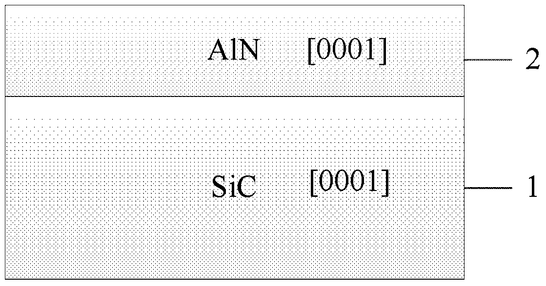
[0036] see figure 1 As shown, the present invention provides a method for obtaining a two-dimensional electron gas in a SiC material, comprising the steps of:
[0037] Step 1: Take a SiC substrate 1 with a crystal plane of (0001), the SiC substrate 1 with a crystal plane of (0001) has a hexagonal wurtzite crystal structure, and the crystal plane is a substrate of (0001) 1 is the crystal plane with zero off angle;
[0038] Step 2: Fabricate an AlN layer 2 with a (0001) crystal plane on a SiC substrate 1 with a (0001) crystal plane.
[0039] Wherein the SiC substrate 1 is a semi-insulating material with a thickness of 3-10 μm, and the thickness of the AlN layer 2 is 5nm-50nm, which can be properly n-type doped to compensate for the loss of two-dimensional electrons at the interface of the two materials. The growth method adopted for the deposited material may be one of chemical vapor deposition, physical vapor deposition, and atomic layer deposition.
Embodiment 2
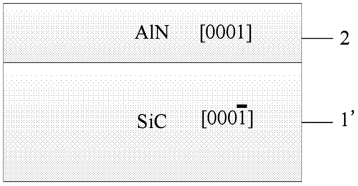
[0041] see figure 2 As shown, the present invention provides a method for obtaining a two-dimensional electron gas in a SiC material, comprising the steps of:
[0042] Step 1: Take a crystal plane as SiC substrate 1, the crystal plane is The SiC substrate 1 has a crystal structure of hexagonal wurtzite, and the crystal planes are The SiC substrate 1 is a crystal plane with zero off-angle;
[0043] Step 2: On the crystal face for An AlN layer 2 with a (0001) crystal plane is fabricated on a SiC substrate 1 .
[0044] Wherein the SiC substrate 1 is a semi-insulating material with a thickness of 3-10 μm, and the thickness of the AlN layer 2 is 5nm-50nm, which can be properly n-type doped to compensate for the loss of two-dimensional electrons at the interface of the two materials. The growth method adopted for the deposited material may be one of chemical vapor deposition, physical vapor deposition, and atomic layer deposition.
Embodiment 3
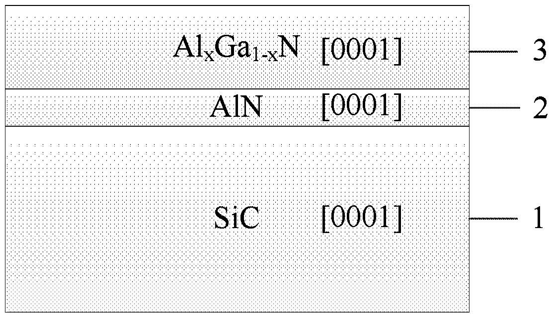
[0046] see image 3 As shown, the present invention provides a method for obtaining a two-dimensional electron gas in a SiC material, comprising the steps of:
[0047] Step 1: Take a SiC substrate 1 with a crystal plane of (0001), the SiC substrate 1 with a crystal plane of (0001) has a hexagonal wurtzite crystal structure, and the crystal plane is a substrate of (0001) 1 is the crystal plane with zero off angle;
[0048] Step 2: making an AlN layer 2 with a (0001) crystal plane on a SiC substrate 1 with a (0001) crystal plane;
[0049] Step 3: Fabricate Al with (0001) crystal plane on the AlN layer 2 with crystal plane (0001) x Ga 1-x N layer 3, the Al x Ga 1-x The Al composition x in the N layer 3 changes from 0 to 1, that is, the material represents one of AlN, AlGaN, and GaN, that is, when x is 0, it is a GaN material, when x is 1, it is an AlN material, and if 0
[0050] Wherein the SiC substrate 1 is a semi-insulating material with a thickness of ...
PUM
| Property | Measurement | Unit |
|---|---|---|
| thickness | aaaaa | aaaaa |
| thickness | aaaaa | aaaaa |
| thickness | aaaaa | aaaaa |
Abstract
Description
Claims
Application Information
 - R&D
- Intellectual Property
- Life Sciences
- Materials
- Tech Scout
- Unparalleled Data Quality
- Higher Quality Content
- 60% Fewer Hallucinations
Browse by: Latest US Patents, China's latest patents, Technical Efficacy Thesaurus, Application Domain, Technology Topic, Popular Technical Reports.
© 2025 PatSnap. All rights reserved.Legal|Privacy policy|Modern Slavery Act Transparency Statement|Sitemap|About US| Contact US: help@patsnap.com