Semiconductor device

Inactive Publication Date: 2007-10-04
NGK INSULATORS LTD
View PDF18 Cites 12 Cited by
  • Summary
  • Abstract
  • Description
  • Claims
  • Application Information

AI Technical Summary

Benefits of technology

[0023]This achieves a semiconductor device serving as a diode having a P—N junction and a Schottky junction in combi

Problems solved by technology

Conventionally practical, silicon-employed P—N junction diode and its modified P-i-N junction diode have advantages of high breakdown voltage at application of a reverse-bias voltage and high output current density at forward conduction because of the occurrence of carrier injection from both P and N sides, but also have a drawback of long reverse recovery time at shutoff, that is, the above requirement (4) is not satisfied.
A SiC-employed Schottky barrier vertical diode as disclosed in the Raghunathan's article achieves the effect of increasing the breakdown voltage unlike a silicon-employed one, however, the drawbacks of not meeting the requirements (1) and (5) have not been solved so far.
SiC single crystal includes many crystal defects (specifically, tubular voids, what is called micropipes) and thus disadvantageously makes it difficult to manufacture with stability a device of relatively large area that can ensure sufficient output current, resulting in poor yields in manufacturing process.
Further, since a SiC-employed P—N junction diode causes carrier recombination resulting from such crystal, the out

Method used


Image

  • Semiconductor device
  • Semiconductor device
  • Semiconductor device

Examples


Example

First Example

[0079]In this example the semiconductor device 10 according to the first preferred embodiment
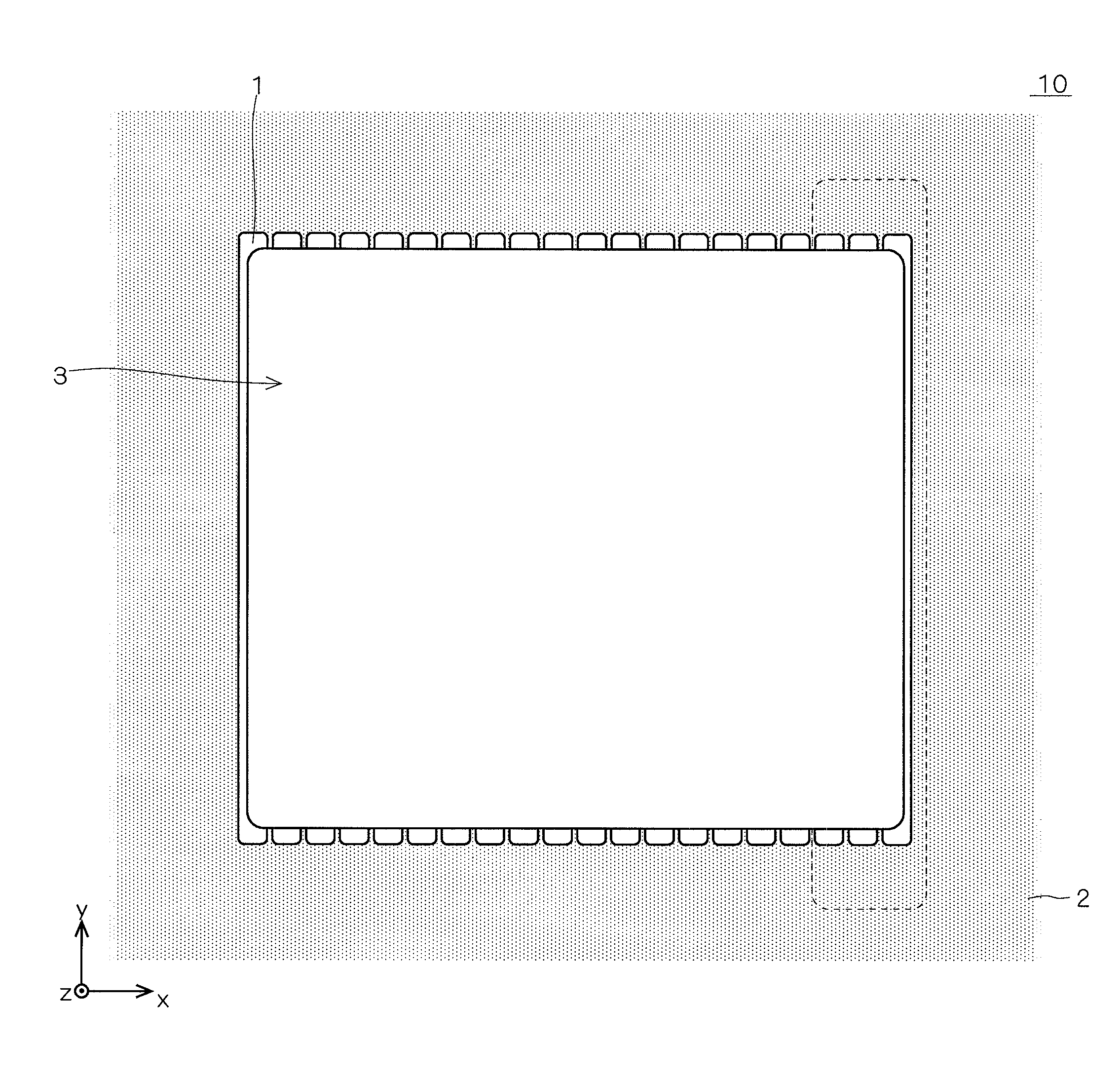
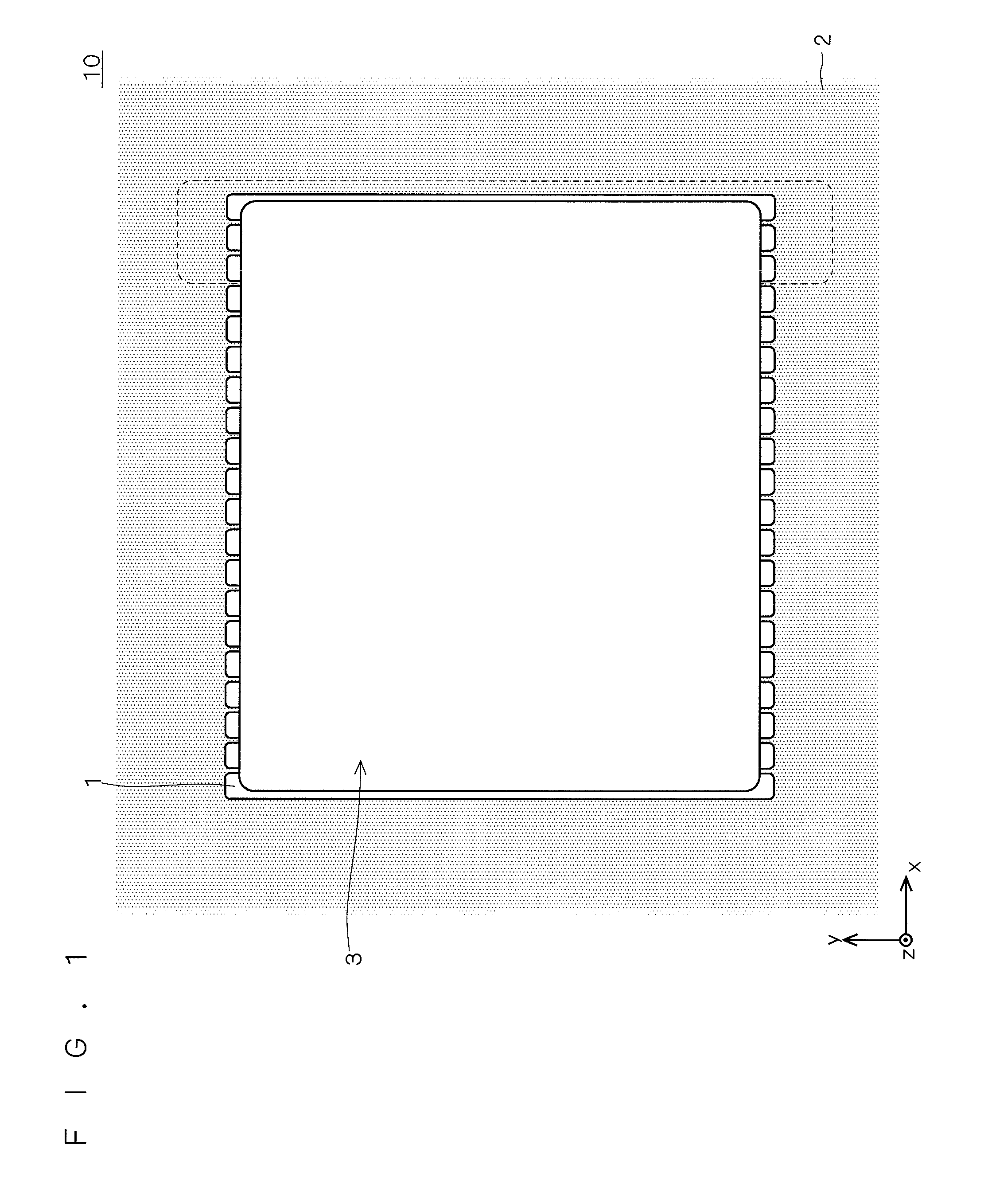
 was prepared, and its properties were evaluated. The conductive layer 1 was manufactured as shown in FIG. 5, with 20 pairs of unit anode portion 5u and unit cathode electrode 2u integrated on one chip.

[0080]First, a GaN layer having a thickness of 3 μm was formed as the first layer 1a on a single crystal SiC substrate by MOCVD with a buffer layer made of AlN having a thickness of 300 nm interposed therebetween, and an Al0.3Ga0.7N layer having a thickness of 20 nm was further formed as the second layer 1b. Electric properties of the conductive layer 1 at this time were evaluated by a Hall coefficient measurement to obtain a two-dimensional electron density of about 1×10¹³ / cm2, an electron mobility of about 1400 cm2 / Vs, and a sheet resistance of about 450 Ω / sq. An X-ray diffraction measurement was conducted to find out that a wurtzite crystal structure was grown sequentially alon...

Example

Second Example

[0085]Processing was conducted similarly to the first example except forming each unit anode portion 5u of Ni layer, to thereby obtain the semiconductor device according to the second preferred embodiment.

[0086]Thus manufactured semiconductor device 10 was measured in leakage current during reverse blocking, reverse blocking breakdown voltage (dielectric breakdown voltage), forward output current, reverse recovery time, peak surge current, on-state voltage at a forward current of 10 A and on-state voltage at a forward current of 1 A.

Example

Third Example

[0087]The semiconductor device 10 was manufactured similarly to the first example except that the conductive layer 1 included the first layer 1a and second layer 1b, and the second layer 1b had a two-layered structure. More specifically, a GaN layer having a thickness of 3 μm was formed as a first layer 1a on a single crystal SiC substrate by MOCVD with a buffer layer made of AlN having a thickness of 300 nm interposed therebetween, then, an AlN layer having a thickness of 1 nm and an Al0.3Ga0.7N layer having a thickness of 20 nm were further formed as the second layer 1b. Electric properties of the conductive layer 1 at this time were evaluated by the Hall coefficient measurement to obtain a two-dimensional electron density of about 1×10¹³ / cm2, an electron mobility of about 2200 cm2 / Vs, and a sheet resistance of about 260 Ω / sq. The X-ray diffraction measurement was conducted to find out that a wurtzite crystal structure was grown sequentially along the c axis.

[0088]Thu...


PUM


Abstract

A semiconductor device made of a group-III nitride semiconductor having excellent properties is provided. The semiconductor device has a horizontal diode structure of Schottky type or P—N junction type, or combined type thereof having a main conduction pathway in the horizontal direction in a conductive layer with unit anode portions and unit cathode electrodes being integrated adjacently to each other in the horizontal direction. The conductive layer is preferably formed by depositing a group-III nitride layer and generating a two-dimensional electron gas layer on the interface. Forming the conductive layer of the group-III nitride having high breakdown field allows the breakdown voltage to be kept high while the gap between electrodes is narrow, which achieves a semiconductor device having high output current per chip area. Further, an electrode pad layer provided on an insulation protecting layer relieves electric field concentration at a junction of each unit anode portion and each unit cathode electrode, which achieves higher breakdown voltage.

Description

FIELD OF THE INVENTION[0001]The present invention relates to a semiconductor device for power applications, and more particularly to a power inverter or converter circuit device.DESCRIPTION OF THE BACKGROUND ART[0002]A semiconductor-employed switching device (transistor, thyristor, etc.) or rectifier device (diode) is widely used as a power inverter or converter circuit device. Under the present circumstances, a more compact device with lower losses is preferable for such semiconductor device for power applications in order to meet future demands for higher power. While silicon has conventionally been used widely as a semiconductor material, wide band gap semiconductor materials having higher breakdown fields are being developed as next-generation semiconductor materials in light of the present circumstances. Since what is called wide band gap semiconductor materials such as diamond, SiC, group-III nitride semiconductor, etc. are expected to have low on-state resistance and high bre...

Claims


Application Information

Patent Timeline
IPC IPC(8): H01L29/00
CPCH01L29/2003H01L29/872H01L29/66462
Inventor MIYOSHI, MAKOTOKURAOKA, YOSHITAKA
Owner NGK INSULATORS LTD
Why Eureka
Try Eureka