Semiconductor device

A semiconductor, conductive type technology, applied in the direction of semiconductor devices, electric solid devices, diodes, etc., can solve the problems of stronger and larger electric field strength, increase of leakage current of diodes, etc., to reduce on-state resistance and suppress leakage current.

Inactive Publication Date: 2012-04-04
KK TOSHIBA
View PDF5 Cites 12 Cited by
  • Summary
  • Abstract
  • Description
  • Claims
  • Application Information

AI Technical Summary

Problems solved by technology

[0006] However, if a Schottky barrier diode is formed in the basic unit cell of a power MOSFET, the cell unit (period of the lateral direction of the cell) in the region where the Schottky junction is formed becomes large.
In a power MOSFET with a field plate structure, when the lateral period becomes longer, the on-state resistance increases
In addition, when the lateral period becomes longer, the electric field strength in the Schottky junction becomes stronger, and the leakage current may increase in the Schottky barrier diode.

Method used


Image

  • Semiconductor device
  • Semiconductor device
  • Semiconductor device

Examples


no. 1 approach

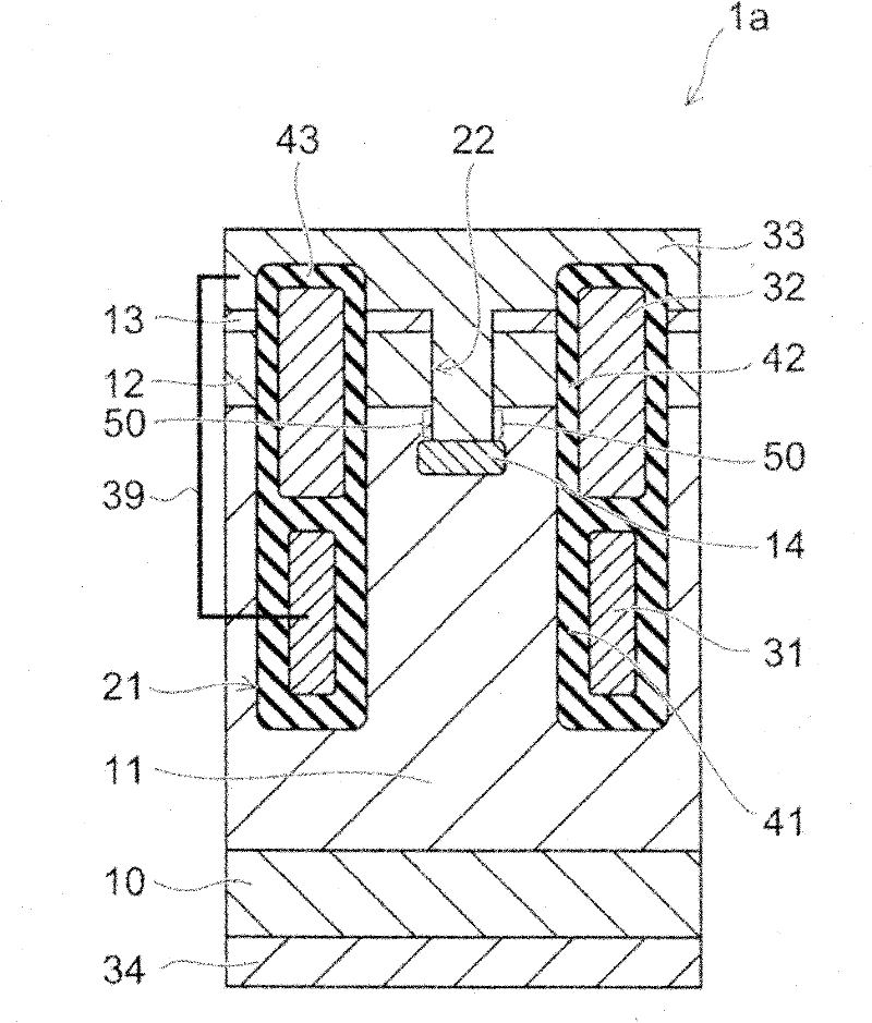
[0025] figure 1 It is a schematic sectional view of a main part of the semiconductor device according to the first embodiment. figure 1 An element portion of a semiconductor device is shown. in the later Figure 2 to Figure 9 in the same way.

[0026] The semiconductor device 1 a includes a power MOSFET having a structure of upper and lower electrodes, and a Schottky barrier diode (hereinafter referred to as SBD). In the semiconductor device 1a, such as figure 1 shown, in n + An n-type drift layer (first semiconductor layer) 11 is provided above the n-type drain layer 10 . A p-type base layer (second semiconductor layer) 12 is formed on the surface of the drift layer 11 . Formed on the surface of the base layer 12 are n + type source layer (third semiconductor layer) 13 . In this embodiment, the embodiment will be described with the drain layer 10 side as the lower side and the source layer 13 as the upper side. That is, the source layer 13 is provided at a shallower ...

no. 2 approach

[0071] Figure 8 It is a schematic cross-sectional view of a main part of the semiconductor device according to the second embodiment.

[0072] Such as Figure 8 As shown, in the semiconductor device 2a, an n-type high-concentration semiconductor layer (fifth semiconductor layer) 15 is provided on the lower side of the base layer 12 in the region A between the trenches 21 and 22. The high-concentration The semiconductor layer 15 contains impurities at a concentration higher than that of the drift layer. The lower end of the high-concentration semiconductor layer 15 is located shallower than the lower end of the guard ring layer 14 . The impurity concentration of the high-concentration semiconductor layer 15 is about several times that of the drift layer 11 . The main component of the high-concentration semiconductor layer 15 is, for example, silicon (Si). In a part of the sidewall of the trench 22 , the metallic source electrode 33 is in contact with the high-concentration...

no. 3 approach

[0080] Figure 10 It is a schematic sectional view of a main part of the semiconductor device according to the third embodiment.

[0081] Figure 10 In FIG. 2 , not only the element region 71 where the MOSFET is formed, but also the termination region 72 from the element region 71 to the outside is shown. That is, the semiconductor device has an element region 71 and a termination region 72 disposed outside the element region 71 around the element region 71 . The element region 71 is a region where the main current path is formed between the drain electrode and the source electrode of the MOSFET, for example, in Figure 10 The middle is a region including the gate electrode 32 and the like. The termination region 72 is a region arranged around the element region 71 on its outer peripheral side, and is a region provided with a field plate electrode 35 , a field insulating film 44 , etc. which will be described later. In the termination region 72 , a field insulating film 44...


PUM


Abstract

The present invention provides a semiconductor device capable of reducing on-resistance of an MOSFET and suppressing leakage current of a Schottky barrier diode. The semiconductor device includes: a first semiconductor layer of a first conductivity type; a second semiconductor layer of a second conductivity type, provided on the first semiconductor layer; a third semiconductor layer of the first conductivity type, provided on the second semiconductor layer; an embedded electrode provided in a first trench via a first insulating film; a control electrode provided above the embedded electrode via a second insulating film in the first trench; a fourth semiconductor layer of the second conductivity type, selectively provided in the first semiconductor layer and connected to a lower end of a second trench; a first main electrode electrically connected to the first semiconductor layer; and a second main electrode provided in the second trench and connected to the second semiconductor layer, the third semiconductor layer and the fourth semiconductor layer. The embedded electrode is electrically connected to one of the second main electrode and the control electrode. A Schottky junction formed of the second main electrode and the first semiconductor layer is formed at a sidewall of the second trench.

Description

[0001] Cross References to Related Applications [0002] This application is based on and claims the benefit of priority from Japanese Patent Application No. 2010-200251 with a filing date of September 7, 2010, the entire contents of which are incorporated herein by reference. technical field [0003] The present invention relates to semiconductor devices. Background technique [0004] As an example of a power semiconductor device, there is a power MOSFET (Metal Oxide Semiconductor Field Effect Transistor: Metal Oxide Semiconductor Field Effect Transistor) having a top and bottom electrode structure. As a means of reducing the on-state resistance of such a power MOSFET, there is a power MOSFET having a field plate structure in which a deep trench is formed in a drift layer and an electrode is filled through an insulating film in the trench. The field plate structure is periodically provided in the drift layer, and the high withstand voltage is maintained by protruding the d...

Claims


Application Information

Patent Timeline
Patent Type & Authority Applications(China)
IPC IPC(8): H01L27/04
CPCH01L29/7813H01L29/402H01L29/66727H01L29/41741H01L29/0619H01L29/7806H01L29/0623H01L29/7811H01L29/407H01L29/0878H01L29/66734H01L29/4236H01L29/42368H01L29/41766H01L29/7839
Inventor 斋藤涉小野升太郎谷内俊治渡边美穗山下浩明
Owner KK TOSHIBA
Why Eureka
Try Eureka