Silicon carbide semiconductor device having junction field effect transistor and method for manufacturing the same

a semiconductor device and junction field technology, applied in the direction of transistors, semiconductor devices, electrical devices, etc., can solve the problems of low on-state resistance and the inability to avoid the problem

Active Publication Date: 2007-06-12
DENSO CORP
View PDF4 Cites 12 Cited by
  • Summary
  • Abstract
  • Description
  • Claims
  • Application Information

AI Technical Summary

Benefits of technology

[0011]In the above constitution, a plurality of channel layers is disposed in each cell of the J-FET. Therefore, when the J-FET is operated, a plurality of channel regions is prepared so that the on-state resistance of the device is reduced even when the maximum voltage applied to a gate of the device is limited.
[0025]The above method provides the silicon carbide semiconductor device, which includes a plurality of channel layers disposed in each cell of the J-FET. Therefore, when the J-FET is operated, a plurality of channel regions is prepared so that the on-state resistance of the device is reduced even when the maximum voltage applied to a gate of the device is limited.

Problems solved by technology

When the normally off type semiconductor device made of silicon carbide is designed, the following points become mainly problems for obtaining a low on-state resistance.
In view of the above points, it is impossible to avoid the problem of No.

Method used


Image

  • Silicon carbide semiconductor device having junction field effect transistor and method for manufacturing the same
  • Silicon carbide semiconductor device having junction field effect transistor and method for manufacturing the same
  • Silicon carbide semiconductor device having junction field effect transistor and method for manufacturing the same

Examples


first embodiment

[0044](First Embodiment)

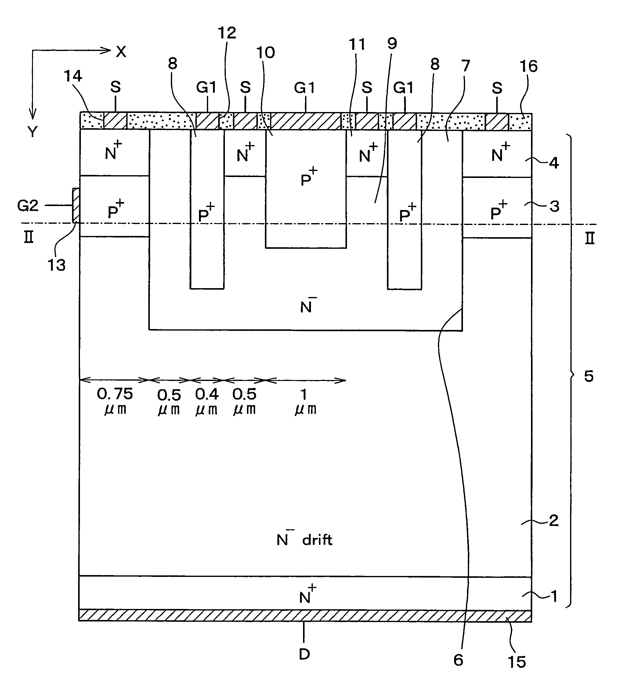
[0045]A silicon carbide semiconductor device according to a first embodiment of the present invention is explained as follows. FIG. 1 is a cross sectional view showing the silicon carbide semiconductor device according to this embodiment. This drawing shows two cells of J-FETs, which are formed in a cell portion of the silicon carbide semiconductor device. As shown in this drawing, each cell is disposed axisymmetrically in a right side or a left side of the drawing. The constitution of the silicon carbide semiconductor device is explained as follows with reference to this drawing.

[0046]As shown in FIG. 1, the silicon carbide semiconductor device includes an N+ conductive type substrate (i.e., a substrate) 1, an N− conductive type drift layer (i.e., the first semiconductor layer) 2, a P+ conductive type layer 3, and an N+ conductive type layer 4. The N+ conductive type substrate 1, the N− conductive type drift layer 2, the P+ conductive type layer 3, and the N...

second embodiment

[0106](Second Embodiment)

[0107]A second embodiment of the present invention is described. FIG. 14 is a cross sectional view showing a silicon carbide semiconductor device according to this embodiment. In the second embodiment, the impurity concentration of the N− conductive type layer 9 is different from the impurity concentration of the N− conductive type epi-layer 7, compared with the first embodiment.

[0108]Specifically, as shown in FIG. 14, the N− conductive type layer 9 shown in FIG. 1 is replaced to an N conductive type layer 20. The impurity concentration of the N− conductive type epi-layer 20 becomes higher than the N− conductive type epi-layer 7. In this case, the inner resistance of the N− conductive type epi-layer 20 can be much reduced so that the on-state resistance is much reduced.

[0109]In the silicon carbide semiconductor device having the above constitution, the deposition process of the N− conductive type epi-layer 9 shown in FIG. 13E is replaced to a deposition proc...

third embodiment

[0111](Third Embodiment)

[0112]A third embodiment of the present invention is described. FIG. 15 is a cross sectional view showing a silicon carbide semiconductor device according to this embodiment. In the third embodiment, the shape of the P+ conductive type layer 8 shown in FIG. 14 is different, compared with the first and second embodiments.

[0113]Specifically, in the silicon carbide semiconductor device according to this embodiment, the P+ conductive type layer 8 is formed not only on a part of the N− conductive type epi-layer 7 disposed on the sidewall of the trench 6 but also on another part of the N− conductive type epi-layer 7 disposed on the bottom of the trench 6. The P+ conductive type layer 8 is separated each other at the center of the N− conductive type epi-layer 7 disposed on the bottom of the trench 6 so that the P+ conductive type layer 8 has a L-shaped cross section shown in FIG. 15.

[0114]When the P+ conductive type layer 8 has the above shape, the electric field is...


PUM


Abstract

A silicon carbide semiconductor device includes a substrate and a junction field effect transistor. The transistor includes: a first semiconductor layer disposed on the substrate; a first gate layer disposed on a surface of the first semiconductor layer; a first channel layer adjacent to the first gate layer on the substrate; a first source layer connecting to the first channel layer electrically; a second gate layer adjacent to the first channel layer to sandwich the first channel layer; a second channel layer adjacent to the second gate layer to sandwich the second gate layer; a third gate layer adjacent to the second channel layer to sandwich the second channel layer; and a second source layer connecting to the second channel layer electrically.

Description

CROSS REFERENCE TO RELATED APPLICATION[0001]This application is based on Japanese Patent Application No. 2003-385094 filed on Nov. 14, 2003, the disclosure of which is incorporated herein by reference.FIELD OF THE INVENTION[0002]The present invention relates to a silicon carbide semiconductor device having a junction field effect transistor and a method for manufacturing the same.BACKGROUND OF THE INVENTION[0003]A semiconductor device having a junction field effect transistor (i.e., a J-FET) in a prior art is disclosed in, for example, Japanese Patent Application Publication No. 2000-312008. The device is shown in FIG. 17. As shown in FIG. 17, the device includes a substrate J4 composed of an N+ conductive type substrate J1, an N− conductive type drift layer J2 and a P+ conductive type first gate layer J3, which are laminated in this order. A trench J5 is formed in the substrate J4 to penetrate the P+ conductive type first gate layer J3. An N− conductive type channel layer J6 and a ...

Claims


Application Information

Patent Timeline
Patent Type & Authority Patents(United States)
IPC IPC(8): H01L29/15H01L21/04H01L29/80H01L21/337H01L29/24H01L29/808
CPCH01L29/1608H01L29/66068H01L29/8083Y10S438/931
Inventor KUMAR, RAJESHMIHAILA, ANDREIUDREA, FLORIN
Owner DENSO CORP
Why Eureka
Try Eureka