
Microwave annealing process

A microwave annealing and process technology, applied in the direction of electrical components, semiconductor/solid-state device manufacturing, circuits, etc., can solve the problems of low efficiency, uneven heating, etc., achieve uniform heat conduction, improve efficiency, and reduce microwave energy.

Inactive Publication Date: 2015-11-11
FUDAN UNIV
View PDF5 Cites 3 Cited by
  • Summary
  • Abstract
  • Description
  • Claims
  • Application Information

AI Technical Summary

Problems solved by technology

However, for non-contact microwave annealing, heat usually needs to be transferred via radiation transfer or conduction of the intermediate atmosphere, which has the problem of low efficiency.
For contact microwave annealing, there may also be problems such as uneven heating due to uneven contact

Method used


Image

  • Microwave annealing process
  • Microwave annealing process
  • Microwave annealing process

Examples


Embodiment Construction

[0026] In order to make the object, technical solution and advantages of the present invention clearer, various embodiments of the present invention will be described in detail below in conjunction with the accompanying drawings. However, those of ordinary skill in the art can understand that, in each implementation manner of the present invention, many technical details are provided for readers to better understand the present application. However, even without these technical details and various changes and modifications based on the following implementation modes, the technical solution claimed in each claim of the present application can be realized.

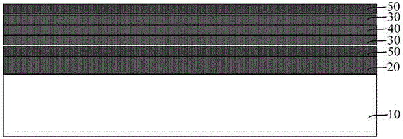
[0027] The first embodiment of the present invention relates to a microwave annealing process, the specific process is as follows figure 1 , which includes the following steps:

[0028] S100: providing a functional layer to be processed;

[0029] S200: forming a high absorption layer on the functional layer;

[0030] S300...


PUM


Abstract

The invention relates to the field of semiconductor manufacturing, and discloses a microwave annealing process. A uniform-covering high absorption layer is formed on a first surface and / or a second surface of a function layer. With the help of high microwave absorption by the high absorption layer, on one hand, uniform heat conduction on the function layer is ensured, and the problem of low non-contact efficiency is overcome; and on the other hand, as the high absorption layer is corresponding to the function layer, the high absorption layer has a tiny mass itself, and the consumed microwave energy is greatly reduced compared with former modes, the energy utilization efficiency is improved.

Description

technical field [0001] The invention relates to the field of semiconductor manufacturing, in particular to a microwave annealing process. Background technique [0002] In the semiconductor manufacturing process, it is usually necessary to use the annealing process multiple times to release stress and activate elements. In addition to the commonly used thermal annealing process, a microwave annealing process is also used in the prior art. [0003] The microwave annealing process is mainly a mechanism in which the material to be annealed absorbs microwaves and converts electromagnetic energy into thermal energy. This mechanism includes: conductance (ohmic) loss, dielectric loss, and magnetic loss. Therefore, microwaves become a means of annealing because they can be absorbed by materials to heat them up. In the early days, this annealing method was mainly used in the synthesis of ceramics and other materials. In recent years, due to the significant reduction in feature size...

Claims


Application Information

Patent Timeline
IPC IPC(8): H01L21/324
CPCH01L21/324
Inventor 付超超吴东平王言
Owner FUDAN UNIV
Learn More