Glass substrate lithography alignment apparatus and aligning method characterized by no positioning marks

A glass substrate and photolithographic alignment technology, which is applied in the direction of electrical components, semiconductor/solid-state device manufacturing, circuits, etc., to achieve the effect of maximizing the effective use area, high-precision photolithographic alignment, and accurate positioning

Active Publication Date: 2015-11-11
BEIJING INST OF CONTROL ENG
View PDF3 Cites 0 Cited by
  • Summary
  • Abstract
  • Description
  • Claims
  • Application Information

AI Technical Summary

Problems solved by technology

[0004] The purpose of the present invention is to overcome the deficiencies of the prior art and provide a photolithography method tha

Method used


Image

  • Glass substrate lithography alignment apparatus and aligning method characterized by no positioning marks
  • Glass substrate lithography alignment apparatus and aligning method characterized by no positioning marks
  • Glass substrate lithography alignment apparatus and aligning method characterized by no positioning marks

Examples


Example Embodiment

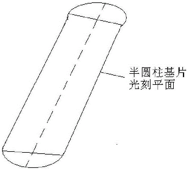
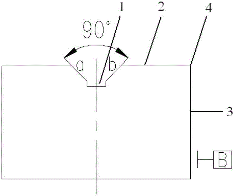
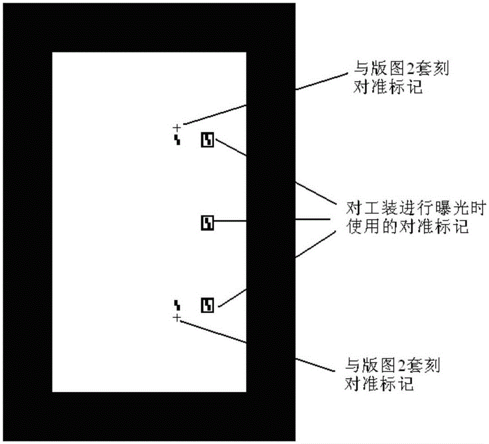
[0043] The present invention provides a set of photoetching masks for photoetching exposure of the positioning tool and the semi-cylindrical glass substrate. In the photolithography method provided in the implementation of the present invention, firstly, a high-precision positioning tool is designed and manufactured to firmly adsorb the substrate during photolithographic exposure of the semi-cylindrical glass substrate. The key dimensions of the tooling are measured, and a set of masks (total of two) are designed according to them. Use one of the masks to make a cross mark on the surface of the tooling by photolithography, and then use the cross mark to align with the cross mark on the other mask, and finally achieve a half without any positioning mark on the surface. The requirements for the alignment accuracy of the lithography of the cylindrical glass substrate are specifically that the deviation (eccentricity) between the center line of the lithographic slit on the plane of...


PUM

PropertyMeasurementUnit
Surface roughnessaaaaaaaaaa

Abstract

The invention relates to a glass substrate lithography alignment apparatus and an aligning method characterized by no positioning marks. A special-purpose positioning tool, a first matching mask and a second matching mask are designed according to the shape of a substrate. A mark is photoetched on the positioning tool through the fist mask. By means of the mark, the positioning of the second mask is achieved. A slit is further photoetched on the glass substrate through a slit of the second mask. The precision of the slit on the glass substrate satisfies that the distance deviation between the actually photoetched slit center line and a semicircular bus is no greater than 3 mu m. Positioning accuracy is achieved. Meanwhile, no destructive marks are formed on the surface of the glass substrate. The effective usable area of the substrate is maximized.

Description

technical field [0001] The invention relates to the technical field of semiconductor manufacturing, in particular to a photolithography method used for photolithography of glass substrates without positioning marks. Background technique [0002] In the manufacture of semiconductor devices, photolithography is a technique for producing geometric figures corresponding to the mask plate on the dielectric film or metal film layer according to the requirements of the device design. The main process of the photolithography process includes steps such as glue coating, pre-baking, exposure, development, and film hardening. The alignment accuracy of the exposure is an important index to determine the photolithography accuracy. [0003] Photolithography in general semiconductor processing technology is to perform exposure alignment with the positioning marks of the standard round silicon wafer itself, or to perform overlay alignment with the alignment marks made on the silicon wafer ...

Claims


Application Information

Patent Timeline
IPC IPC(8): H01L21/68H01L21/67
CPCH01L21/67282H01L21/682
Inventor 赵娜朱春英曾宪沪秦素然刘江赵晓雨石建民
Owner BEIJING INST OF CONTROL ENG
Why Eureka
Try Eureka