Staggered heterojunction tunneling field effect transistor based on InAsN-GaAsSb material

A tunneling field effect and transistor technology, applied in semiconductor devices, electrical components, circuits, etc., can solve the problems of inability to form staggered heterojunctions, difficulty in meeting performance requirements, and small conduction current, so as to improve conduction current, increase tunneling probability, and improve device performance

Active Publication Date: 2015-11-11
XIDIAN UNIV
View PDF4 Cites 8 Cited by
  • Summary
  • Abstract
  • Description
  • Claims
  • Application Information

AI Technical Summary

Problems solved by technology

Currently available TFETs made of common III-V materials, because they cannot form a staggered heterojunction, the tunneling probability is low, resulting in a small conduction current, and it is difficult to meet the performance requirements

Method used


Image

  • Staggered heterojunction tunneling field effect transistor based on InAsN-GaAsSb material
  • Staggered heterojunction tunneling field effect transistor based on InAsN-GaAsSb material

Examples


Embodiment 1

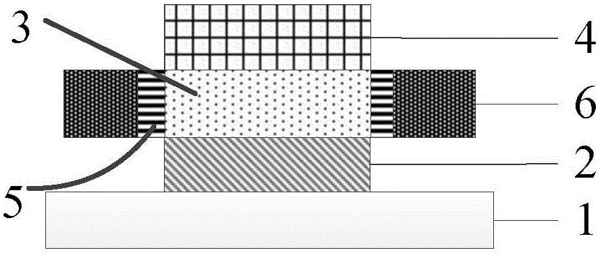
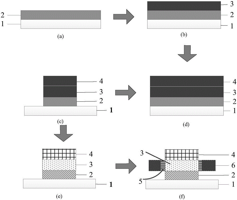
[0031] Embodiment 1: Making InAs-based 0.95 N 0.05 -GaAs 0.35 Sb 0.65 Materials for staggered heterojunction n-channel tunneling field effect transistors.

[0032] Step a: Using molecular beam epitaxy, on the InAs substrate 1, using solid In, As and N as evaporation sources, at a temperature of 725°C and a pressure of 10 -4 Pa conditions, grow the InAsN composite material with N composition of 0.05 to form the source layer, such as figure 2 a.

[0033] Step b: Using molecular beam epitaxy, on the source layer, using solid Ga, As and Sb as evaporation sources, at a temperature of 725°C and a pressure of 10 -4 Pa condition, grow GaAsSb composite material with Sb composition of 0.65 to form a channel layer, such as figure 2 b;

[0034] Step c: Using molecular beam epitaxy, on the channel layer, using solid Ga, As and Sb as evaporation sources, at a temperature of 725°C and a pressure of 10 -4 Pa condition, grow the GaAsSb composite material with Sb composition of 0.65 t...

Embodiment 2

[0041] Embodiment 2: Making InAs-based 0.97 N 0.03 -GaAs 0.5 Sb 0.5 Materials for staggered heterojunction p-channel tunneling field effect transistors.

[0042] Step 1: Using molecular beam epitaxy, on an InAs substrate 1, using solid In, As and N as evaporation sources, at a temperature of 725°C and a pressure of 10 -4 Pa condition, grow the InAsN composite material with N composition of 0.03 to form the source layer, such as figure 2 a;

[0043] Step 2: Using molecular beam epitaxy, on the source layer, use solid Ga, As and Sb as evaporation sources at a temperature of 725°C and a pressure of 10 -4 Pa conditions, grow GaAsSb composite material with Sb composition of 0.5 to form a channel layer, such as figure 2 b;

[0044] Step 3: Using molecular beam epitaxy, on the channel layer, use solid Ga, As and Sb as evaporation sources at a temperature of 725°C and a pressure of 10 -4 Pa condition, grow the GaAsSb composite material with Sb composition of 0.5 to form the dr...

Embodiment 3

[0052] Embodiment 3: Making InAs-based 0.99 N 0.01 -GaAs 0.65 Sb 0.35 Staggered Heterojunction P-Channel Tunneling Field-Effect Transistor Based on Materials

[0053] The first step: using molecular beam epitaxy, on the InAs substrate 1, using solid In, As and N as evaporation sources, at a temperature of 725°C and a pressure of 10 -4 Pa conditions, grow the InAsN composite material with N composition of 0.01 to form the source layer, such as figure 2 a;

[0054] The second step: using molecular beam epitaxy, on the source layer, using solid Ga, As and Sb as evaporation sources, at a temperature of 725 ° C and a pressure of 10 -4 Pa conditions, grow GaAsSb composite material with Sb composition of 0.35 to form a channel layer, such as figure 2 b;

[0055] The third step: using molecular beam epitaxy, on the channel layer, using solid Ga, As and Sb as evaporation sources, at a temperature of 725°C and a pressure of 10 -4 Pa condition, grow the GaAsSb composite materia...


PUM


Abstract

The invention discloses a staggered heterojunction tunneling field effect transistor based on an InAsN-GaAsSb material, and mainly aims at solving the problem that an existing field effect transistor prepared from the III-V material is relatively low in on-state current. The staggered heterojunction tunneling field effect transistor comprises a substrate (1), a source (2), a channel (3), a drain (4), an insulating dielectric film (5) and a gate electrode (6); an InAsN composite material in which an N component is 0-0.05 is adopted by the source; a GaAsSb composite material in which an Sb component is 0.35-0.65 is adopted by the channel and the drain; and the source, the channel and the drain are vertically distributed on the substrate from bottom to top. The source InAsN material and the channel GaAsSb material contact with each other to form a staggered tunneling heterojunction, so that the low-tunneling barrier height is effectively reduced; the tunneling probability and the tunneling current are increased; the whole performance of the device is improved; and the staggered heterojunction tunneling field effect transistor can be applied to fabrication of large-scale integrated circuits.

Description

technical field [0001] The invention belongs to the technical field of microelectronic devices, in particular to a staggered heterojunction tunneling field effect transistor, which can be used in large-scale integrated circuits. Background technique [0002] With the development of integrated circuits, the feature size of chips has been continuously reduced, and the integration level on a single chip has increased accordingly, and the resulting power consumption problem has become more and more serious. According to ITRS data, when the feature size is reduced to the 32nm node, the power consumption will be 8 times the expected trend, that is, with the gradual reduction of the feature size, traditional MOS devices will not be able to meet the performance requirements in terms of power consumption. In addition, the reduction of MOSFET size is limited by the minimum subthreshold swing of 60mv / decade at room temperature. However, compared with the MOSFET, the tunneling field ef...

Claims


Application Information

Patent Timeline
Patent Type & Authority Applications(China)
IPC IPC(8): H01L29/78H01L29/205H01L29/08H01L29/10
CPCH01L29/0843H01L29/1025H01L29/2003H01L29/205H01L29/78
Inventor 韩根全张春福彭悦汪银花张进城郝跃
Owner XIDIAN UNIV
Why Eureka
Try Eureka