Time-domain hardened latch capable of resisting dual-node upset

A dual-node inversion and latch technology, applied in electrical components, logic circuits, pulse technology, etc., can solve problems such as few reports and inability to resist single-event pulses

Inactive Publication Date: 2015-11-18
TIANJIN UNIV
View PDF5 Cites 3 Cited by
  • Summary
  • Abstract
  • Description
  • Claims
  • Application Information

AI Technical Summary

Problems solved by technology

However, there are few reports about
Existing latches that are resistant to MBUs are either proposed under the assumption that a single radiation particle does not cause simultaneous flipping of sensitive nodes in different wells, or are not resistant to single event pulses (Single event Transient, SET) on the input signal

Method used


Image

  • Time-domain hardened latch capable of resisting dual-node upset
  • Time-domain hardened latch capable of resisting dual-node upset
  • Time-domain hardened latch capable of resisting dual-node upset

Examples


Embodiment Construction

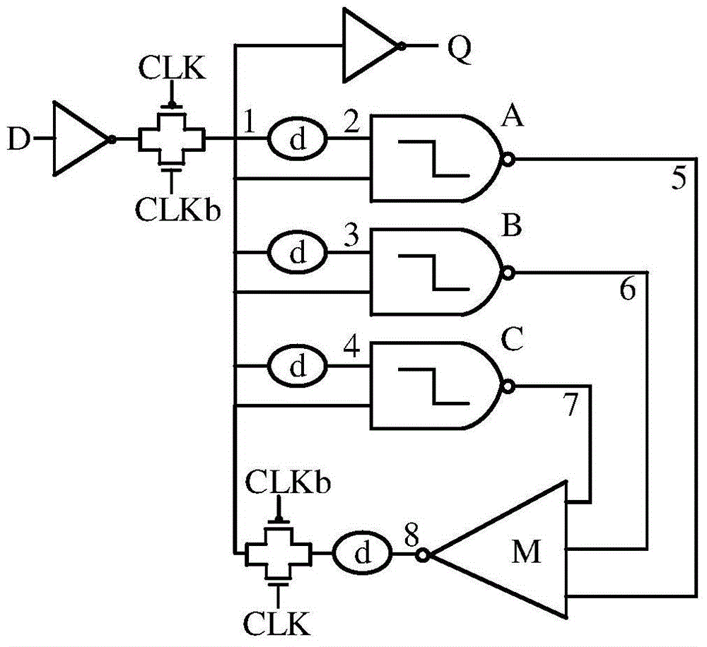
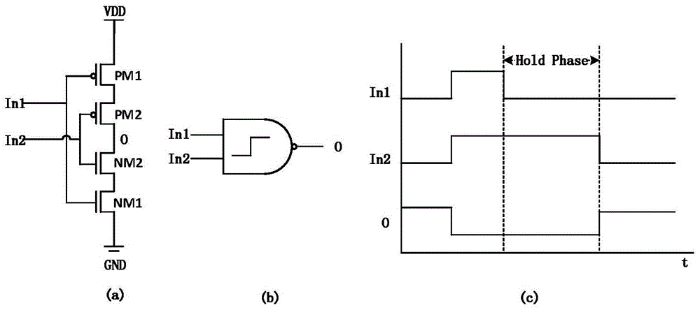
[0013] use as figure 1 The circuit configuration shown. The latch is composed of 3 double-input protection gates (DoubleInputGuard_gate, DIG), 4 delay units, 2 transmission gates, 2 inverters and 1 three-select two-way multiplexer. The node 1 after the input D passes through an inverter and a low-level conduction transmission gate, and the node 2 after it passes through the first delay unit are jointly used as the input of DIGA. 1 and its node 3 after the second delay unit are used as the input of DIGB. 1 and its node 4 after the third delay unit are used as the input of DIGC. The output nodes of A, B, and C are 5, 6, and 7 in turn, and they are also the input of the three-to-two multiplexer, and the output nodes are 8, 8. After the fourth delay unit and a high-level conduction transmission Feedback to 1 node behind the gate. Node 1 is connected to an inverter and then output, and the output node is Q. Since one of the inputs of DIG is delayed for a certain time, the effe...


PUM


Abstract

The invention relates to the field of radiation-hardened integrated circuit design, and provides a latch capable of resisting dual-node upset, which not only can resist dual-node upset, but also can resist SET on an input line and SET on a clock line, and enables a storage state of a latch to be changeless. Therefore, by the adoption of the technical scheme, the latch capable of resisting the dual-node upset is composed of three double input guard gates (Double Input Guard-gate, DIG), four delay units, two transmission gates, two inverters and one two-out-of-three multiplexer; after an input D passes through one inverter and one low-level conduction transmission gate, the node is 1, and after the node 1 passes through a first delay unit, the node is 2; the node 1 and the node 2 are commonly taken as an input of a first double input guard gate. The latch capable of resisting the dual-node upset is mainly applied to designing and manufacturing radiation-hardened integrated circuits.

Description

technical field [0001] The invention relates to the field of anti-radiation integrated circuit design, in particular, the design adopts time domain redundancy and space redundancy technology to reinforce the sequential circuit. So that the sequential circuit has the ability to resist single event upset (Single eventupset, SEU) and multiple bit upset (Multiple-bitupsets, MBUs). Specifically, it involves time-domain hardened latches that are resistant to double-node flipping. technical background [0002] For digital circuits used in space environments, especially sequential circuits, the occurrence of single event upsets (Single event upset) will seriously affect the correctness of chip functions. With the reduction of the size of the integrated circuit and the reduction of the chip power supply voltage, the probability of multiple-bit flips (Multiple-bitupsets) is gradually increasing, thereby affecting the performance of the circuit. [0003] For SEU protection, circuit d...

Claims


Application Information

Patent Timeline
Patent Type & Authority Applications(China)
IPC IPC(8): H03K19/094
Inventor 徐江涛闫茜聂凯明高志远姚素英高静史再峰
Owner TIANJIN UNIV
Why Eureka
Try Eureka