

A resistive variable memory using a metamaterial electrode structure and its preparation method
A technology of resistive variable memory and electrode structure, applied in the direction of electrical components, etc., can solve the problems that cannot fully meet the requirements of the development of non-volatile memory, and achieve the effect of enriching applications
- Summary
- Abstract
- Description
- Claims
- Application Information
AI Technical Summary
Problems solved by technology
Method used
Image

Examples
Embodiment 1
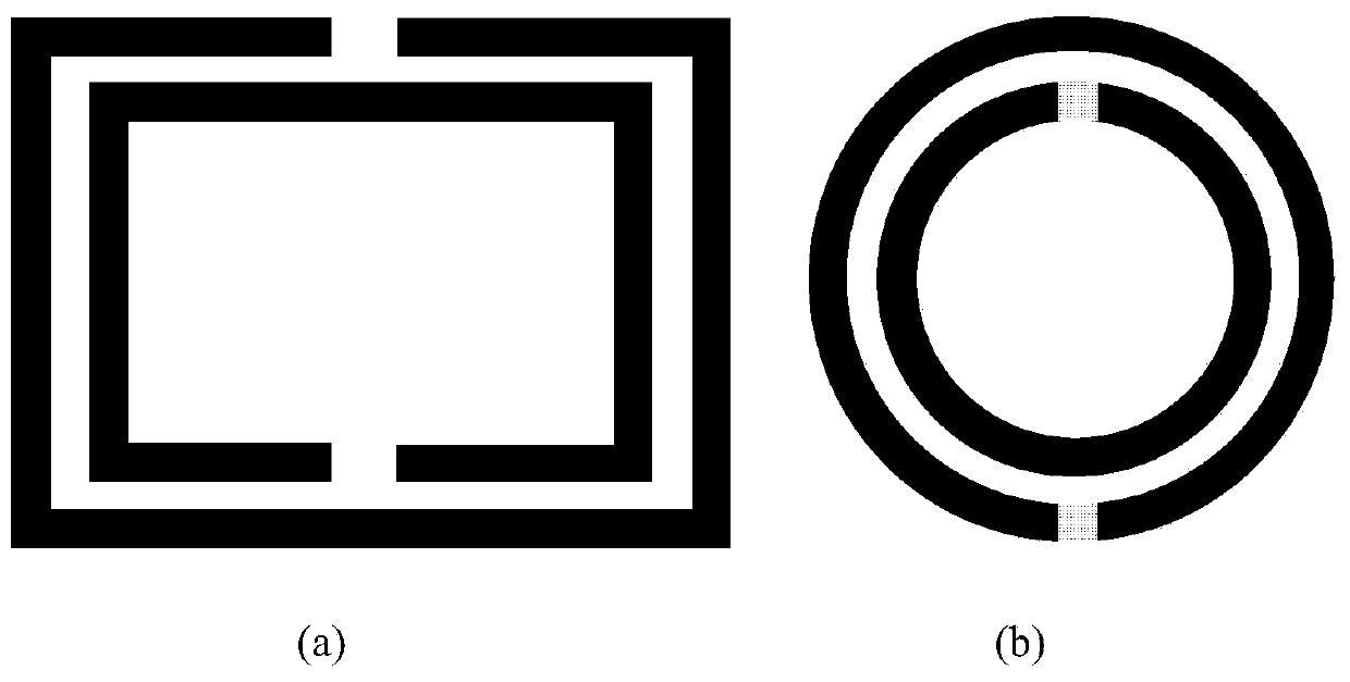
[0029] Embodiment 1 (SRR and derived structures are used as metamaterial electrodes as examples):
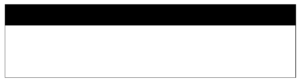
[0030] 1) A layer of resistive thin film material is grown on the Si substrate, such as figure 2 Shown:
[0031] 1.1) Prepare a layer of resistive thin film material by CVD reactive sputtering method:
[0032] Specific materials can be TaOx, HfOx, Al2O3, SiOx, TiOx, etc., with a thickness between 20nm and 50nm; image 3 shown.
[0033] 1.2) ALD (Atomic layer deposition) method is used to deposit thinner resistive film materials: specific materials can be TaOx, HfOx, Al2O3, etc., with a thickness between 5-10nm.
[0034] The above provides two different methods for preparing resistive thin film materials, ie, sputtering and ALD methods, both of which have their own advantages. The performance of the resistive thin film material prepared by ALD deposition method will be better, and it is more suitable for depositing thinner films. The ALD deposition method is equivalent to th...
Embodiment 2
[0040] Embodiment 2 (SRR and derived structures are used as metamaterial electrodes as examples):
[0041] 1) A layer of resistive thin film material is grown on the Si substrate, such as figure 2 Shown:
[0042] This step is the same as step 1) in Example 1, and will not be described in detail.
[0043] 2) Coating a layer of photoresist on the resistive thin film layer, such as Figure 5 shown.
[0044] 3) Forming an electrode pattern on the photoresist on the resistive film material by photolithography of a mask.
[0045] In this embodiment, the electrode pattern structure is an SRR structure, and the pattern formed in this step includes the SRR structure pattern and the macroscopic pattern of the electrode.
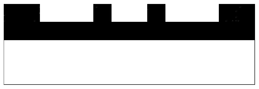
[0046] 4) Etch the resistive thin film layer to a thickness of 5nm-50nm by using the AME etching technology of the semiconductor CMOS process, such as Image 6 shown. The resistive material layer is etched to expose the substrate.
[0047] 5) Metal metamaterial e...
PUM
 Abstract
Description
Claims
Application Information