

Radiation-resistant latch based on three-input protective gate
A protection gate, three-input technology, applied in the field of circuit design, anti-radiation integrated circuit design, can solve the problems of increasing circuit delay and power consumption, increasing circuit area, etc., to achieve the effect of reducing circuit area and power consumption
- Summary
- Abstract
- Description
- Claims
- Application Information
AI Technical Summary
Problems solved by technology
Method used
Image

Examples
Embodiment Construction
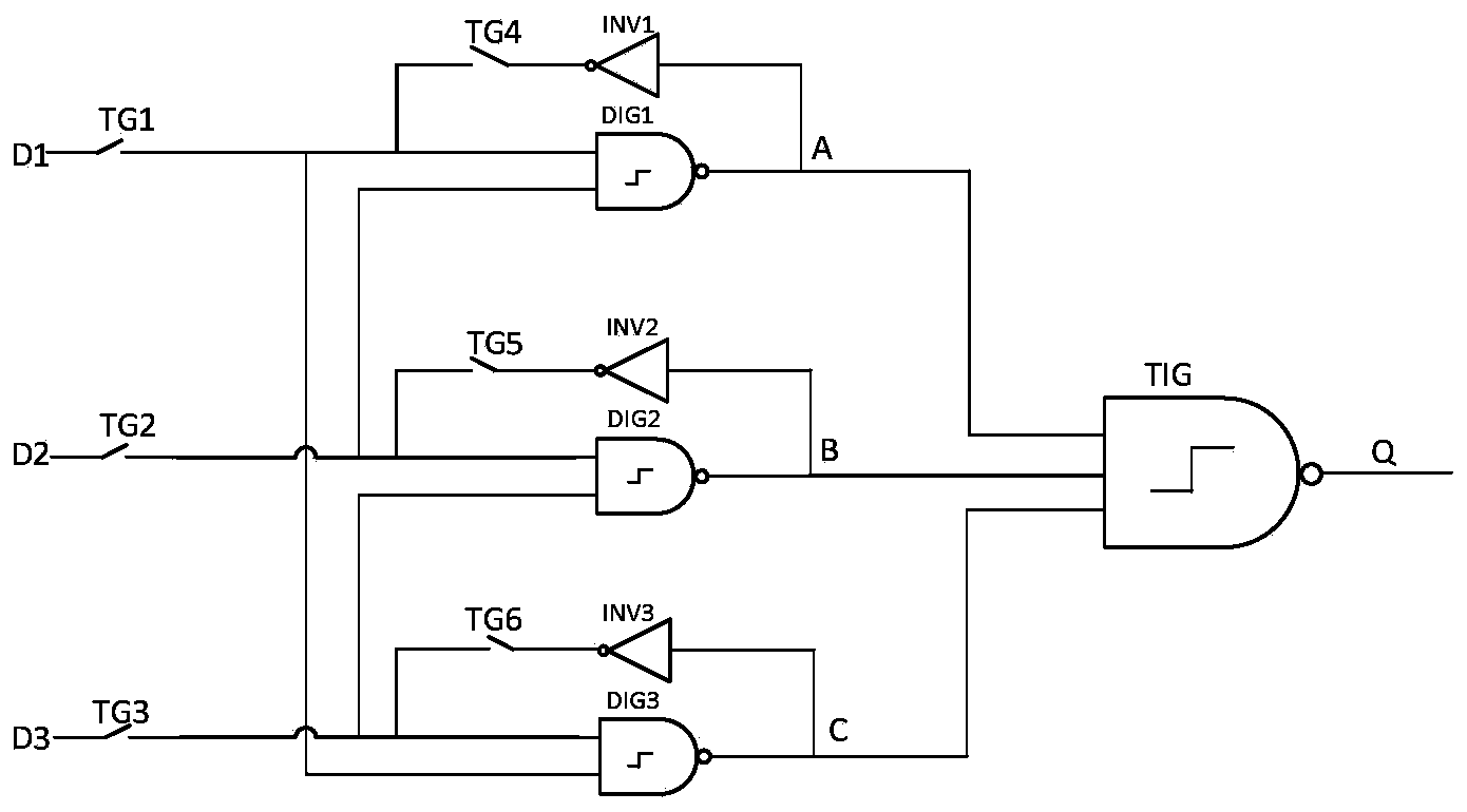
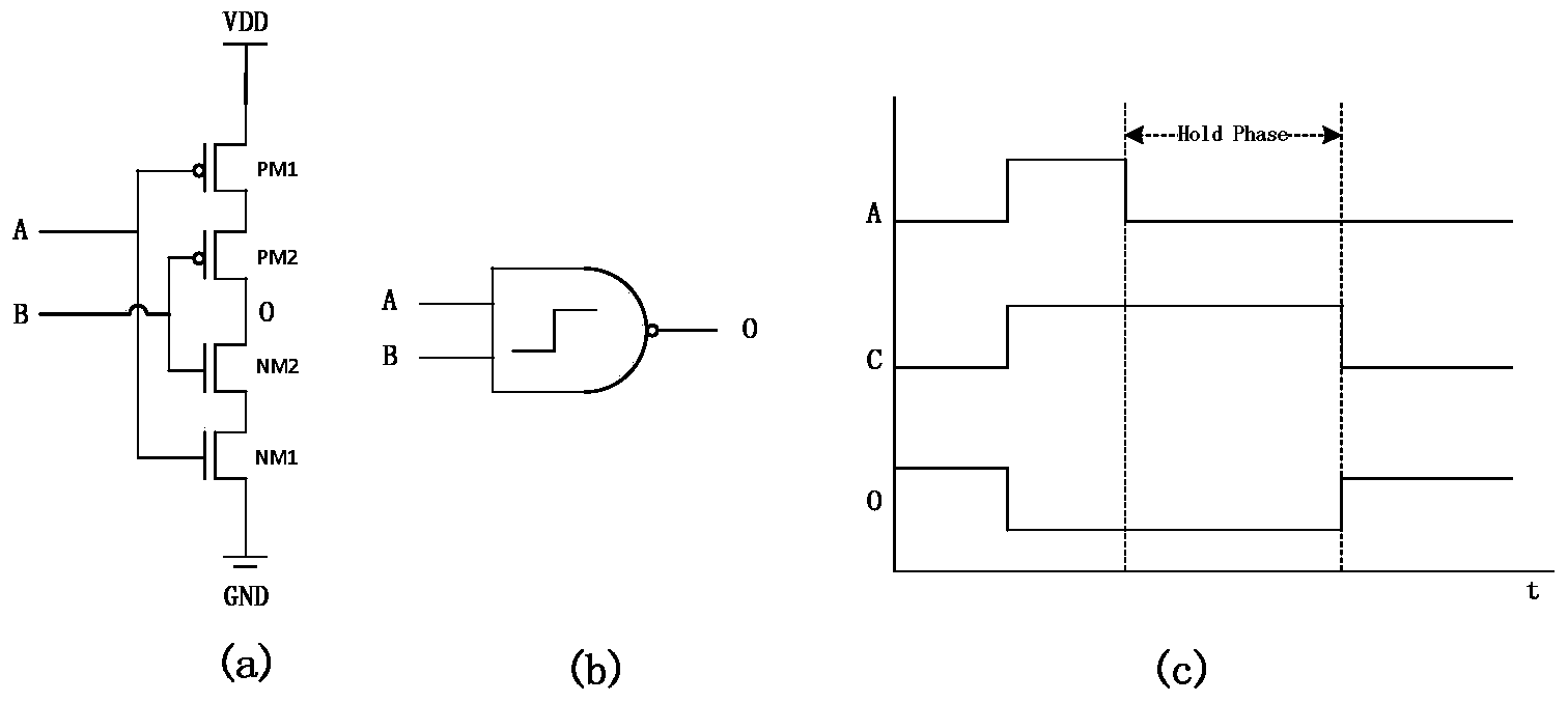
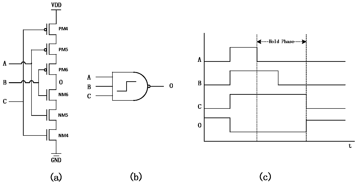
[0014] use as figure 1 The circuit configuration shown. The latch structure includes 6 transmission gates TG1~6, 3 inverters INV1~3, 3 double input guard gates (Double Input Guardgate, DIG) DIG1~3 and a triple input guard gate (Trible Input Guardgate, TIG). It has three identical input signals D1, D2, and D3, which are sent to the latch through switches TG1, TG2, and TG3 respectively. D1 and D2 are used as the input of DIG1, and the output A of DIG1 is connected to one of its input terminals D1 through an inverter INV1 and a switch TG4. Similarly, D2 and D3 are used as the input of DIG2, and the output B is connected to D2 through the inverter INV2 and TG5. D1 and D3 are used as the input of DIG3, and the output C is connected to D3 through the inverter INV3 and TG6. A, B, and C are used as input signals of TIG, and Q is output. where DIG (such as figure 2 (a) shows its transistor-level structure, (b) its logic symbol, (c) its timing diagram) using two PMOS and two NM...
PUM
 Abstract
Description
Claims
Application Information