led filament and filament led bulbs
A technology of LED filament and LED chip, applied in lighting and heating equipment, electrical components, circuits, etc., can solve the problems of component failure, the conductive pin 15 of the LED filament falling off, breaking and other problems, so as to increase the bonding strength and increase the bonding area. Effect
- Summary
- Abstract
- Description
- Claims
- Application Information
AI Technical Summary
Problems solved by technology
Method used
Image
Examples
no. 1 example
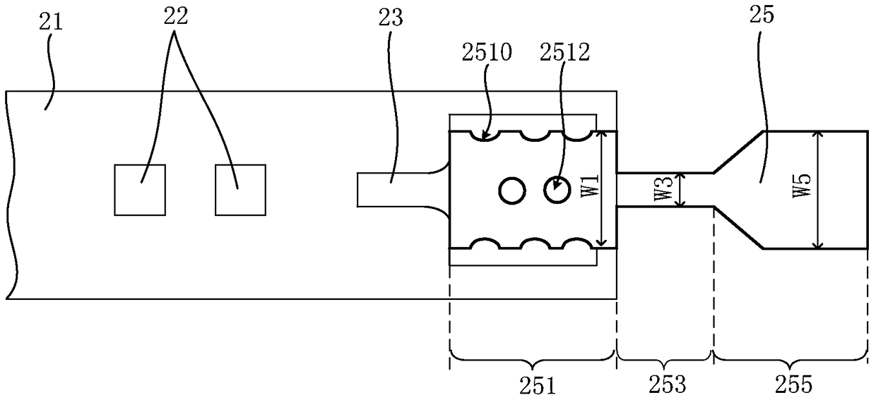
[0033] See Figure 2A , The LED filament provided by the first embodiment of the present invention includes: a carrier 21 , a plurality of LED chips 22 arranged on the carrier 21 , and conductive pins 25 fixedly connected to the carrier 21 . Wherein, the carrier 21 is used to carry the LED chip 22, which is, for example, a light-transmitting material such as transparent ceramics, sapphire or glass substrate; a plurality of LED chips 22 are connected in series, parallel or series-parallel, and are usually fixed on the carrier 21. Each LED chip 22 can form an electrical connection through a metal wire and be connected to a conductive electrode 23 pasted or printed on the carrier 21, where the conductive electrode 23 is, for example, a silver conductive pad (Ag pad); 25 is electrically connected with a plurality of LED chips 22 to provide external power to a plurality of LED chips 22, which includes a pin head 251, a pin tail 255, and a pin neck connecting the pin head 251 and th...
no. 2 example
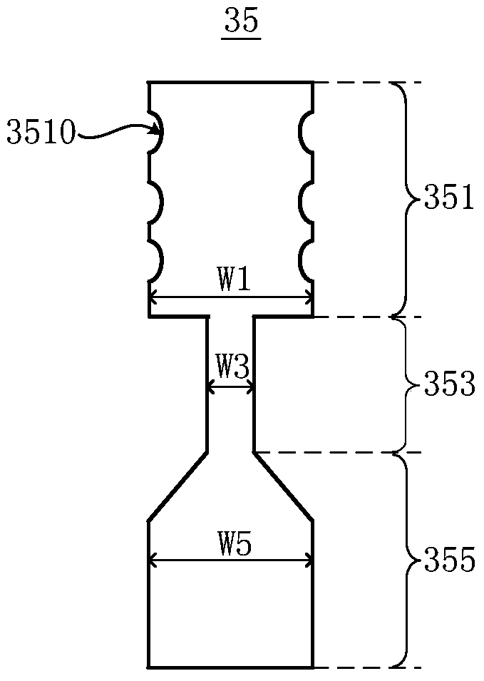
[0036] See Figure 2B A conductive pin 35 for LED filament provided by the second embodiment of the present invention includes: a pin head 351, a pin tail 355, and a pin neck 353 connecting the pin head 351 and the pin tail 355, The pin head 351 , the pin neck 353 and the pin tail 355 are typically of an integral structure.
[0037]Both sides of the pin head 351 are provided with arc-shaped recesses 3510 , so that the bonding area between the pin head 351 and the carrier 21 can be increased, thereby increasing the bonding strength between the pin head 351 and the carrier 21 . The two sides of the pin neck 353 are retracted relative to the pin head 351, that is, the pin neck 353 is retracted in the width direction relative to the pin head 351, so as to reduce the physical width of the pin neck 353 And become the weak point of the conductive pin 35 . The two sides of the pin tail portion 355 are not retracted relative to the pin head 351 , and neither side is provided with a r...
no. 3 example
[0039] See Figure 2C A conductive pin 45 for LED filament provided by the third embodiment of the present invention includes: a pin head 451, a pin tail 455, and a pin neck 453 connecting the pin head 451 and the pin tail 455, The pin head 451 , the pin neck 453 and the pin tail 455 are typically integral structures.
[0040] The two sides of the pin head 451 are provided with arc-shaped recesses 4510 and the middle part is provided with a circular through hole 4512, so that the bonding area between the pin head 451 and the carrier 21 can be increased, thereby increasing the distance between the pin head 451 and the carrier 21. Then intensity. The two sides of the pin neck 453 and the two sides of the pin tail 455 are all retracted relative to the pin head 451, that is, the pin neck 453 and the pin tail 455 are at a width relative to the pin head 451. The overall shrinkage in the direction reduces the physical width of the pin neck 453 and becomes the weak point of the cond...
PUM
 Abstract
Description
Claims
Application Information


