Liquid crystal display panel and antistatic array substrate thereof

A liquid crystal display panel and array substrate technology, applied in the direction of nonlinear optics, instruments, optics, etc., can solve the problems of large pressure difference, increase the frame width of the liquid crystal display panel, unfavorable narrow frame design, etc., so as to reduce static electricity accumulation and benefit narrow Frame design, reduce the effect of wiring

Inactive Publication Date: 2015-11-25
TCL CHINA STAR OPTOELECTRONICS TECH CO LTD
View PDF5 Cites 2 Cited by
  • Summary
  • Abstract
  • Description
  • Claims
  • Application Information

AI Technical Summary

Problems solved by technology

In order to prevent the voltage difference between the scanning line 11 and the data line 12 from being too large, the line width of the common electrode line 14 is made very wide to red

Method used


Image

  • Liquid crystal display panel and antistatic array substrate thereof
  • Liquid crystal display panel and antistatic array substrate thereof
  • Liquid crystal display panel and antistatic array substrate thereof

Examples


Example Embodiment

[0024] The technical solutions in the embodiments of the present invention will be described clearly and completely with reference to the accompanying drawings in the embodiments of the present invention. Obviously, the described embodiments are only a part of the embodiments of the present invention, not all the embodiments. Based on the embodiments of the present invention, all other embodiments obtained by those of ordinary skill in the art without creative work shall fall within the protection scope of the present invention.
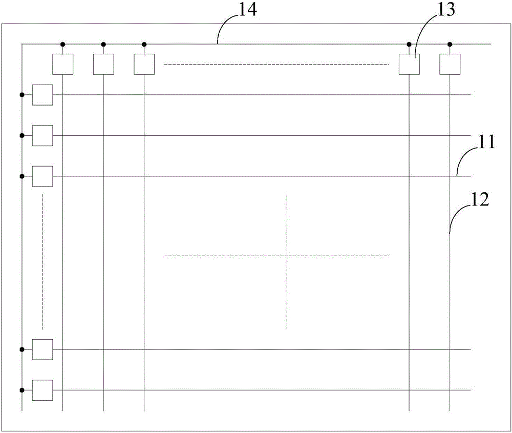
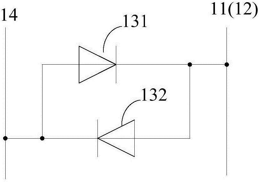
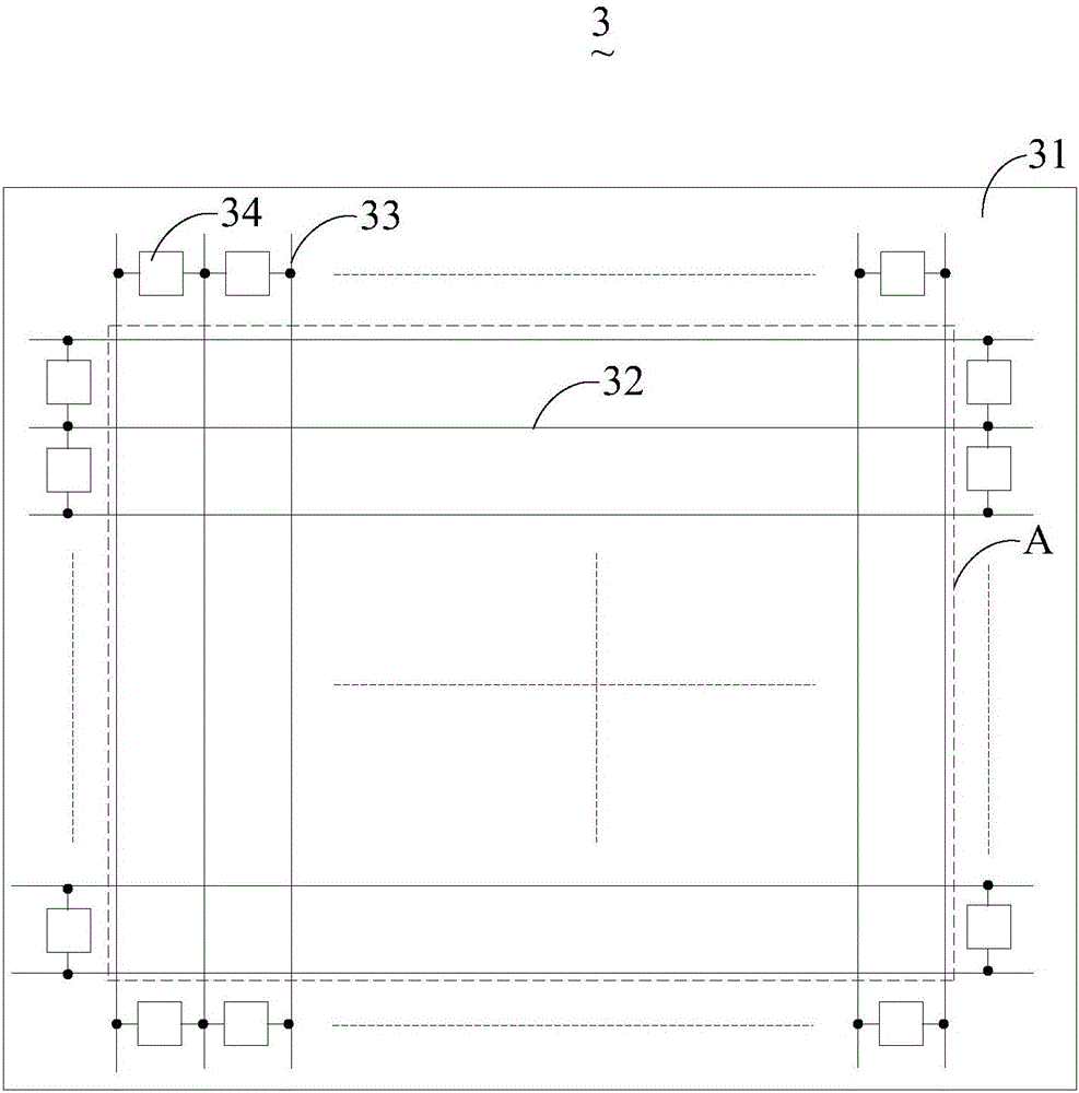
[0025] See image 3 As shown, image 3 It is a schematic diagram of the structure of the array substrate of the first embodiment of the present invention. Such as image 3 As mentioned, the array substrate 3 disclosed in this embodiment includes a substrate 31, a plurality of scan lines 32, a plurality of data lines 33 and a plurality of first antistatic circuits 34.

[0026] A plurality of scan lines 32 and a plurality of data lines 33 are intersected an...


PUM


Abstract

The invention discloses a liquid crystal display panel and an antistatic array substrate thereof. The array substrate comprises a substrate, a plurality of scanning lines, a plurality of data lines and a plurality of first antistatic circuits. The scanning lines and the data lines are intersected on the substrate to define a display area. One first antistatic circuit is arranged between every two adjacent scanning lines or data lines, so that every two adjacent scanning lines or data lines discharge electricity to each other through the corresponding first antistatic circuit. In this way, static electricity accumulation can be reduced.

Description

technical field [0001] The invention relates to the technical field of liquid crystal display, in particular to a liquid crystal display panel and an antistatic array substrate thereof. Background technique [0002] Due to the complicated manufacturing process of the liquid crystal display panel, static electricity is easily generated, which leads to the breakdown and damage of the thin film transistor, which seriously affects the yield and quality of the liquid crystal display panel. [0003] Such as figure 1 As shown, the antistatic liquid crystal display panel in the prior art includes a plurality of scanning lines 11, a plurality of data lines 12, a plurality of antistatic circuits 13 and common electrode lines 14, and each scanning line 11 and each data line 12 are The antistatic circuit 13 is connected to the common electrode line 14 so that both the scanning line 11 and the data line 12 are discharged through the antistatic circuit 13 and the common electrode line 14...

Claims


Application Information

Patent Timeline
IPC IPC(8): G02F1/1362G02F1/1368
CPCG02F1/136204G02F1/136286G02F1/1368
Inventor 曹尚操
Owner TCL CHINA STAR OPTOELECTRONICS TECH CO LTD
Why Eureka
Try Eureka