A liquid crystal display device and gate drive circuit thereof

A technology of gate drive circuit and liquid crystal display device, which is applied to static indicators, instruments, etc., can solve the problem that the thin film transistor of the shift register circuit cannot be turned off normally, and achieve the effect of avoiding abnormal operation and improving the turn-off performance.

Active Publication Date: 2018-04-10
TCL CHINA STAR OPTOELECTRONICS TECH CO LTD
View PDF5 Cites 0 Cited by
  • Summary
  • Abstract
  • Description
  • Claims
  • Application Information

AI Technical Summary

Problems solved by technology

When the low voltages of clock signals CK1 and CK2, selection signals LC1 and LC2, and voltage reference signal VSS are all VGL, the thin film transistors of the shift register circuit cannot be turned off normally.

Method used


Image

  • A liquid crystal display device and gate drive circuit thereof
  • A liquid crystal display device and gate drive circuit thereof
  • A liquid crystal display device and gate drive circuit thereof

Examples


Embodiment Construction

[0025] The following will clearly and completely describe the technical solutions in the embodiments of the present invention in conjunction with the accompanying drawings in the embodiments of the present invention. Obviously, the described embodiments are only some of the embodiments of the present invention, not all of them. Based on the embodiments of the present invention, all other embodiments obtained by persons of ordinary skill in the art without making creative efforts belong to the protection scope of the present invention.

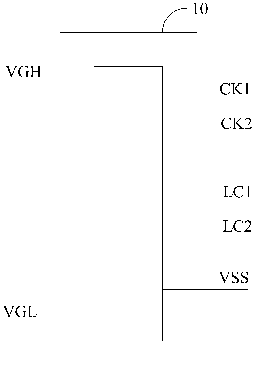
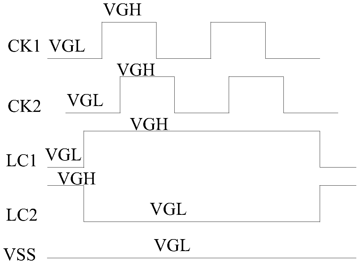
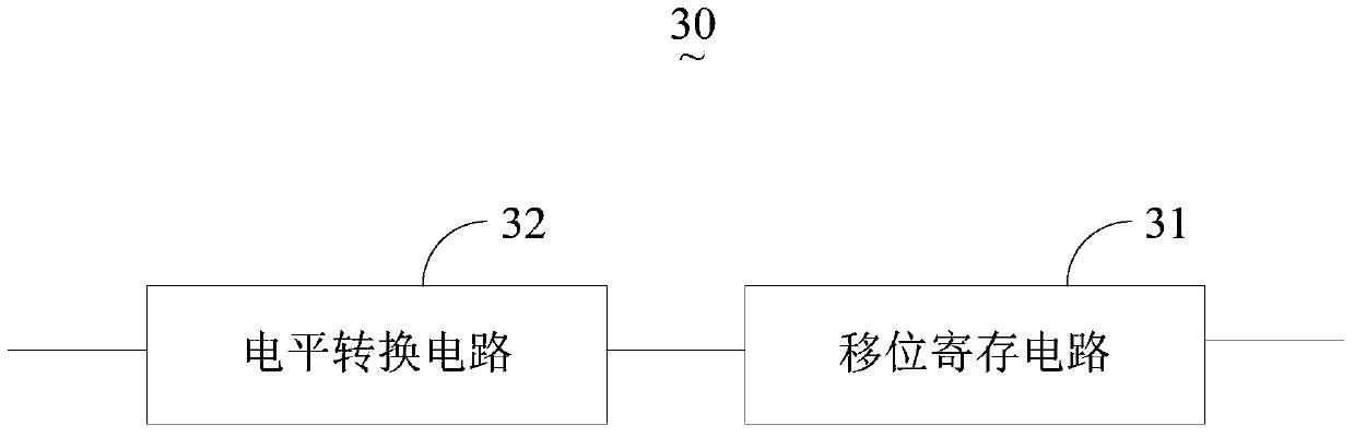
[0026] See image 3 as shown, image 3 is a block diagram of the gate drive circuit of the first embodiment of the present invention. The gate driving circuit disclosed in this embodiment is applied to a liquid crystal display device. Such as image 3 As shown, the gate driving circuit 30 includes a level conversion circuit 32 and a shift register circuit 31 connected to the level conversion circuit 32 . Wherein, the level conversion circui...


PUM


Abstract

A LCD and the gate driving circuit thereof are disclosed. The gate driving circuit includes a shift register circuit and a shift register circuit and a level transition circuit connected with the shift register circuit. The level transition circuit generates clock signals, selection signals, and negative voltage reference signals for the shift register circuit. The clock signals, the selection signals, and the negative voltage reference signals are configured for driving the shift register circuit. A negative voltage value of the negative voltage reference signals (VSS) is larger than the negative voltage value of one of the clock signals or the selection signals. In this way, the TFTs of the shift register circuit own better turn-off capability so as to avoid malfunction.

Description

technical field [0001] The invention relates to the technical field of liquid crystal display, in particular to a liquid crystal display device and a gate driving circuit thereof. Background technique [0002] See Figure 1-2 as shown, figure 1 is a circuit diagram of a level conversion circuit in the prior art, figure 2 yes figure 1 The timing diagram of the clock signal, select signal and voltage reference signal in the figure. Such as figure 1 As shown, the prior art level conversion circuit 10 is used to generate clock signals CK1 and CK2, selection signals LC1 and LC2, and voltage reference signal VSS, and clock signals CK1 and CK2, selection signals LC1 and LC2, and voltage reference signal VSS are used for Drive the shift register circuit. Among them, the input high voltage VGH and low voltage VGL of the level conversion circuit 10, the high voltages of the clock signal CK1, the clock signal CK1, the selection signal LC1 and the selection signal LC2 are all V...

Claims


Application Information

Patent Timeline
Patent Type & Authority Patents(China)
IPC IPC(8): G09G3/36
CPCG09G3/3677G09G3/3696G09G2300/0871G09G2310/0286G09G2310/08
Inventor 张华
Owner TCL CHINA STAR OPTOELECTRONICS TECH CO LTD
Why Eureka
Try Eureka