Integrated structure of IGZO transistor and GaN HEMT grid control circuit and preparation method thereof

A technology of transistors and circuits, which is applied in the field of preparation of the above-mentioned integrated structures, can solve problems such as insufficient performance and excellent compound semiconductors, and achieve the effects of good thermal conductivity, saving and controlling power consumption, and enhancing heat dissipation

Pending Publication Date: 2022-03-04
西安电子科技大学芜湖研究院
View PDF0 Cites 1 Cited by
  • Summary
  • Abstract
  • Description
  • Claims
  • Application Information

AI Technical Summary

Problems solved by technology

However, Si-based integrated circuits also have their limitations, and their performance in some aspects is not as good as that of compound semiconductors.
In the prior art, there are few double-channel IGZO transistors used in low-voltage control circuits

Method used


Image

  • Integrated structure of IGZO transistor and GaN HEMT grid control circuit and preparation method thereof

Examples


Embodiment 1

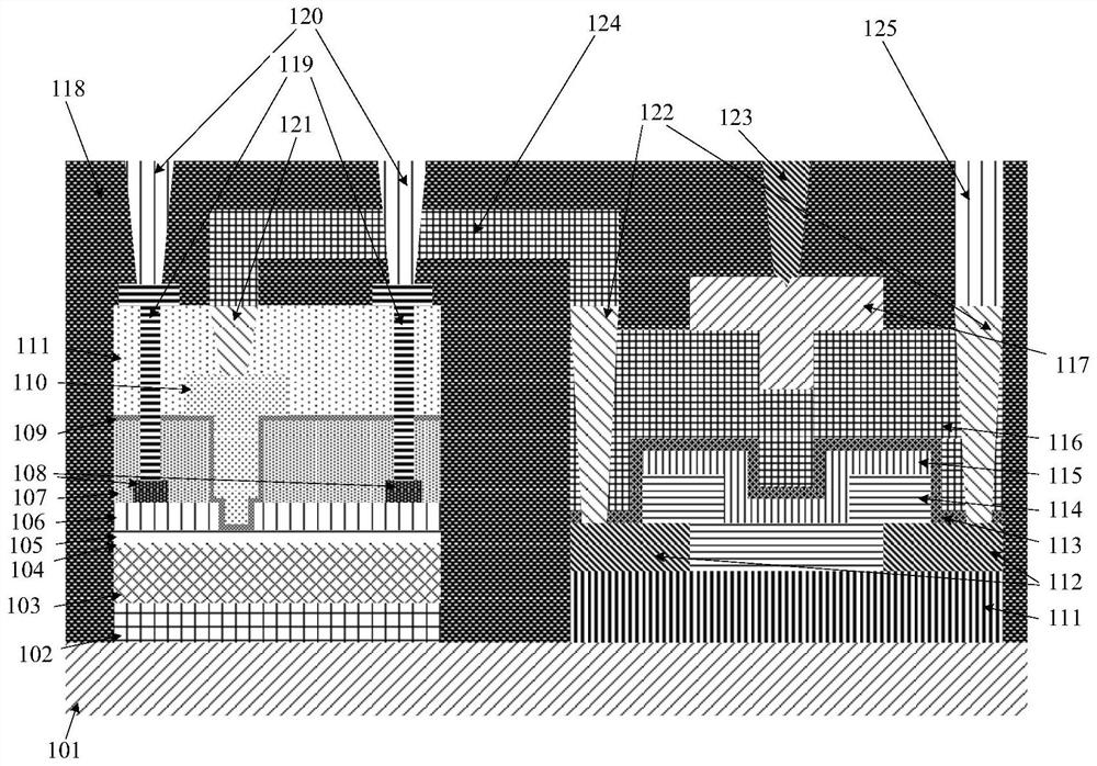
[0048] (1) A thicker SiN layer 118 is grown on the substrate 101, and then etched in the corresponding GaN HEMT device position area to form a concave hole;

[0049] (2) On the basis of the above structure, the AlGaN buffer layer 102 is grown by metal-organic chemical vapor deposition;

[0050] (3) Unintentionally doping and growing a GaN buffer layer 103 on the basis of the above structure by metal-organic chemical vapor deposition method or other methods, with a thickness of 1 μm;

[0051] (4) The AlN layer 104 is formed by unintentional doping growth on the basis of the above structure by metal-organic source chemical vapor deposition;

[0052] (5) Using metal-organic source chemical vapor deposition method to form Al by unintentional doping and growth on the basis of the above structure 0.2 Ga 0.8 N layer 105;

[0053] (6) The AlGaN layer 106 is formed by unintentional doping and growth on the basis of the above structure by metal-organic source chemical vapor depositio...

Embodiment 2

[0069] The rest is the same as that of Embodiment 1, except that the thickness of the GaN buffer layer 103 in step (3) is 100 nm.

Embodiment 3

[0071] The rest is the same as that of Embodiment 1, except that the thickness of the GaN buffer layer 103 in step (3) is 10 um.


PUM

PropertyMeasurementUnit
thicknessaaaaaaaaaa
thicknessaaaaaaaaaa
thicknessaaaaaaaaaa

Abstract

The invention discloses an integrated structure of an IGZO transistor and a GaN HEMT grid-control circuit and a preparation method of the integrated structure, and relates to the technical field of semiconductors, the integrated structure is divided into two parts, one part is a GaN HEMT structure, the other part is an IGZO transistor, the two parts are both grown on a substrate (101), and the IGZO transistor and the GaN HEMT grid-control circuit are arranged on the substrate (101). On the basis of growth of a GaN HEMT, an IGZO transistor and a diamond substrate, the invention provides an integrated grid control circuit structure in which a low-voltage control circuit, the IGZO transistor is used for controlling the high-power GaN HEMT and the IGZO transistor and the high-power GaN HEMT are integrated on one substrate, a GaN HEMT device is a high-power device, and how to dissipate heat to ensure normal work of the GaN HEMT device is a hot research problem. The diamond material is good in heat-conducting property and is introduced as the substrate, so that the heat dissipation capability of the device and the circuit can be better enhanced.

Description

technical field [0001] The invention belongs to the technical field of semiconductors, and in particular relates to an integrated structure of an IGZO transistor and a GaN HEMT gate control circuit and a preparation method of the integrated structure. Background technique [0002] Similar to gallium nitride (GaN), diamond and silicon carbide (SiC), the third-generation semiconductor material with a wide band gap (WideBand Gap Semiconductor, referred to as WBGS). Among them, gallium nitride (GaN) has wide band gap, direct band gap, high breakdown field strength, low dielectric constant, high saturation electron drift velocity, good radiation resistance and good chemical stability, so Become a research and application hotspot. AlGaN / GaN HEMT devices have many advantages, mainly including high breakdown voltage, low on-resistance, etc., so it is considered by the industry as an excellent power switching device or power electronic device. Under high temperature, high power, hi...

Claims


Application Information

Patent Timeline
Patent Type & Authority Applications(China)
IPC IPC(8): H01L27/06H01L29/78H01L29/778H01L21/335H01L21/84H01L21/34
CPCH01L27/0617H01L21/84H01L29/7787H01L29/66462H01L29/78H01L29/66969
Inventor 李彦佐陈兴王东吴勇黄永陈瑶林长志邱慧嫣谢雨峰
Owner 西安电子科技大学芜湖研究院
Why Eureka
Try Eureka