Array substrate and preparation method thereof

An array substrate and substrate technology, which is applied in the field of array substrates and their preparation, can solve the problems of complex preparation process of the array substrate, and achieve the effects of reducing the number of patterning processes, having good transmission performance and simplifying the preparation method.

Active Publication Date: 2015-11-25
BOE TECH GRP CO LTD
View PDF3 Cites 13 Cited by
  • Summary
  • Abstract
  • Description
  • Claims
  • Application Information

AI Technical Summary

Problems solved by technology

[0003] The present invention aims at the problem that the preparation process of the existing array substrate using double-channel thin film transistors is complex, and provides an array substrate that can simplify the preparation process and a preparation method thereof

Method used


Image

  • Array substrate and preparation method thereof
  • Array substrate and preparation method thereof
  • Array substrate and preparation method thereof

Examples


Embodiment 1

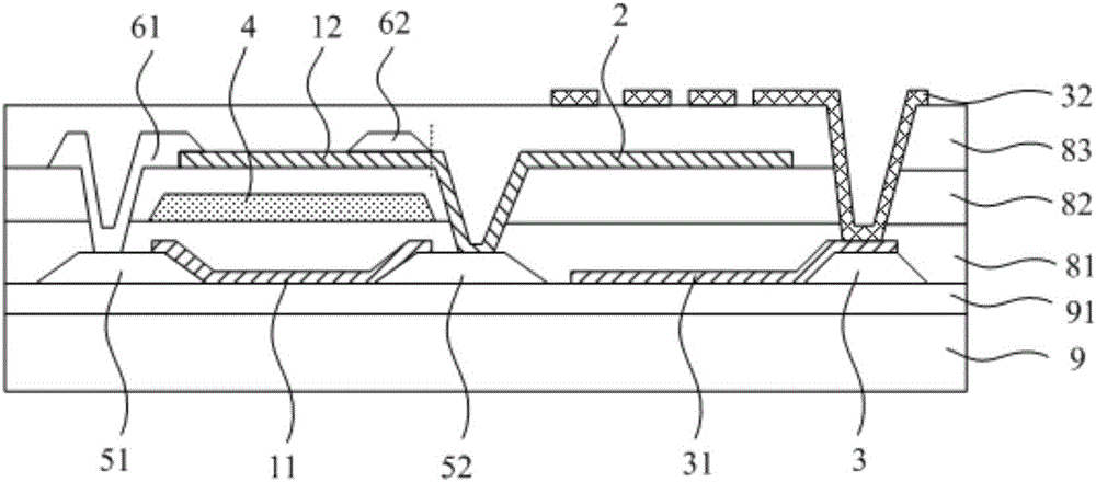
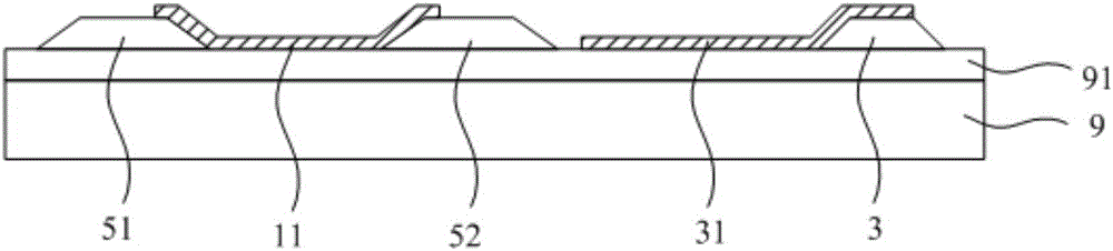
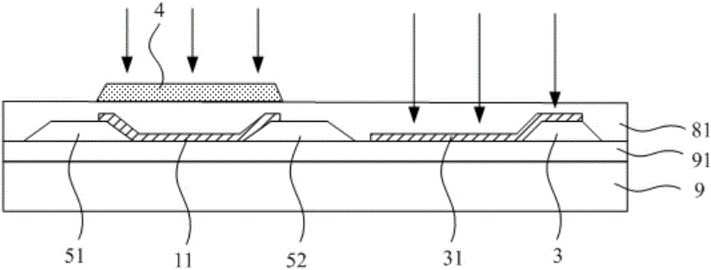
[0032] Such as Figure 1 to Figure 7 As shown, this embodiment provides an array substrate, which includes:

[0033] A plurality of thin film transistors, the thin film transistors include: a gate 4; a first active region 11 and a second active region 12 made of metal oxide semiconductors respectively located below and above the gate 4;

[0034] a first electrode on the same layer as the first active region 11;

[0035] A second electrode on the same layer as the second active region 12;

[0036] Wherein, the first electrode and the second electrode are made of ion-implanted metal oxide semiconductor.

[0037] Preferably, the metal oxide semiconductor is gallium indium zinc oxide (IGZO), indium tin zinc oxide (ITZO), zinc tin oxide (TZO), indium zinc oxide (IZO), aluminum indium oxide (AIO), yttrium zinc oxide (YZO ), zinc oxide (ZnO), indium oxide (InO) in any one.

[0038] Of course, the two active regions (and corresponding electrodes) can be made of the same material, ...

Embodiment 2

[0089] This embodiment provides a display device, which includes any one of the above-mentioned array substrates.

[0090] Specifically, the display device can be any product or component with a display function such as a liquid crystal display panel (because it has a common electrode), an electronic paper, a mobile phone, a tablet computer, a television set, a monitor, a notebook computer, a digital photo frame, and a navigator.


PUM


Abstract

The invention provides an array substrate and a preparation method thereof, belongs to the technical field of array substrates, and aims at solving the problem of complicated preparation technology of the existing array substrate employing a double-channel thin-film transistor. The array substrate provided by the invention comprises a plurality of thin-film transistors, a first electrode and a second electrode, wherein each thin-film transistor comprises a grid, a first active region and a second active region; each first active region and each second active region are respectively located below and above each grid and are composed of metal-oxide semiconductors; the first electrode and the first active regions are located on the same layer; the second electrode and the second active regions are located on the same layer; and the first electrode and the second electrode are composed of ion-implanted metal-oxide semiconductors.

Description

technical field [0001] The invention belongs to the technical field of array substrates, and in particular relates to an array substrate and a preparation method thereof. Background technique [0002] In the array substrate of the liquid crystal display device, the performance of the thin film transistor has an important influence on the final display performance. In order to improve the charging capacity of thin film transistors, one way is to adopt a "double channel" structure, that is, active regions are provided above and below the gate (of course, there is a gate insulating layer between the two active regions and the gate) , thereby simultaneously charging the pixel electrode through the two active regions. However, the additional active region requires a separate patterning process, which complicates the fabrication process of the double-channel thin film transistor. Contents of the invention [0003] The present invention aims at the problem that the preparation ...

Claims


Application Information

Patent Timeline
Patent Type & Authority Applications(China)
IPC IPC(8): H01L27/12H01L29/786H01L21/77
Inventor 胡合合宁策
Owner BOE TECH GRP CO LTD
Why Eureka
Try Eureka