Small-size printed circuit board (PCB) clamping device

A technology of PCB board and clamping device is applied in the field of PCB board manufacturing process, which can solve the problem of taking up a lot of process time, and achieve the effects of improving mass production efficiency, reasonable structure and convenient board placement.

Inactive Publication Date: 2015-11-25
HEFEI ADVANTOOLS SEMICON
View PDF7 Cites 5 Cited by
  • Summary
  • Abstract
  • Description
  • Claims
  • Application Information

AI Technical Summary

Problems solved by technology

If a small piece of PCB is exposed, the time for load...

Method used


Image

  • Small-size printed circuit board (PCB) clamping device
  • Small-size printed circuit board (PCB) clamping device

Examples


Embodiment approach

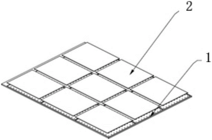
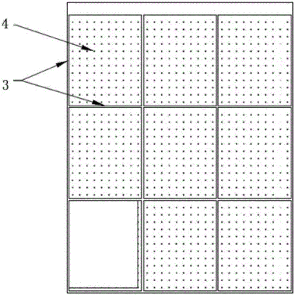
[0021] Before the small PCB board exposure processing, the small PCB board according to figure 1 The array shown is placed on the special clamping device, and placed according to the position of the initial positioning edge. A total of 9 small boards can be placed, and the special clamping device with 9 small boards placed on the suction cup of the LDI equipment , turn on the vacuum. At this time, the suction cup vacuum absorbs the small-sized PCB board through the through hole of the special clamping device, completes the fixing of the PCB, and then performs PCB exposure processing, and then closes the suction cup vacuum after the processing is completed, removes the special clamping device, and puts another piece on it. The special fixture device for the PCB board reciprocates in this way to complete the exposure of a large number of small-sized PCB boards.


PUM


Abstract

The invention discloses a small-size printed circuit board (PCB) clamping device, which comprises a clamping structure, wherein limiting sides are arranged on the clamping structure; the surface of the clamping structure is divided into a plurality of PCB placement regions through the limiting sides; the PCB placement regions are used for placing PCBs; through holes are formed in the surfaces of various PCB placement regions; the other ends of the through holes are connected with a vacuum-pumping device; and the vacuum-pumping device finishes adsorption of the PCBs on the PCB placement regions through exhausting the through holes. The small-size PCB clamping device is reasonable in structure; board placement is facilitated; and the mass production efficiency of the small-size PCBs is greatly improved.

Description

technical field [0001] The invention relates to the field of PCB board manufacturing process, in particular to a device for clamping a PCB board. Background technique [0002] LDI is a laser direct imaging device, which is a key device in the PCB board manufacturing process. The usual LDI processing capacity can process a PCB board with a size of 610mm*800mm, and the time for placing the board at one time is about 6s. A processing time is about 12s. If a small piece of PCB is exposed, the time for loading and unloading the board will take up a lot of process time. At this time, it is necessary to improve work efficiency. There is a need for a special fixture device that can hold many small-sized PCB boards at one time to save time for loading and unloading boards. Contents of the invention [0003] In order to solve the above technical problems, the present invention provides a small-sized PCB board clamping device, which includes a clamping structure, the clamping str...

Claims


Application Information

Patent Timeline
IPC IPC(8): H05K3/00
CPCH05K3/0008H05K2203/0195H05K2203/15
Inventor 张磊王晓光
Owner HEFEI ADVANTOOLS SEMICON
Why Eureka
Try Eureka