Exposure device and method

The technology of an exposure device and an exposure method is applied in the field of photolithography, which can solve the problems such as the reduction of exposure accuracy and product performance, increase the exposure process time, long exposure time, etc., so as to improve the exposure accuracy and product performance, shorten the exposure delay time, The effect of shortening the exposure time

Inactive Publication Date: 2009-06-17
SEMICON MFG INT (SHANGHAI) CORP
View PDF1 Cites 7 Cited by
  • Summary
  • Abstract
  • Description
  • Claims
  • Application Information

AI Technical Summary

Problems solved by technology

[0012] The above bipolar exposure process will increase the time required for the exposure process due to the need to switch the reticle and calibrate the positions of the two reticles separately. Furthermore, it will take longer to perform bipolar exposure on multiple wafers. exposure time, thus reducing production efficiency
And the increase of the exposure time will increase the post-

Method used


Image

  • Exposure device and method
  • Exposure device and method
  • Exposure device and method

Examples


Embodiment Construction

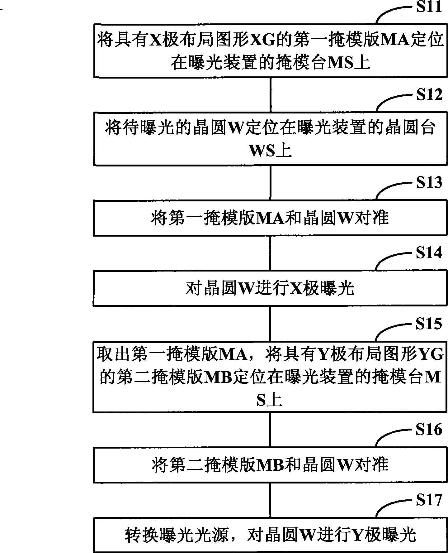
[0049] In the embodiment of the present invention, the first reticle with the layout pattern in the first direction and the second reticle with the layout pattern in the second direction are placed on the mask table at the same time, so that only the first reticle, the second reticle Align once with the mask stage respectively. The specific implementation manners of the present invention will be described in detail below in conjunction with the accompanying drawings.

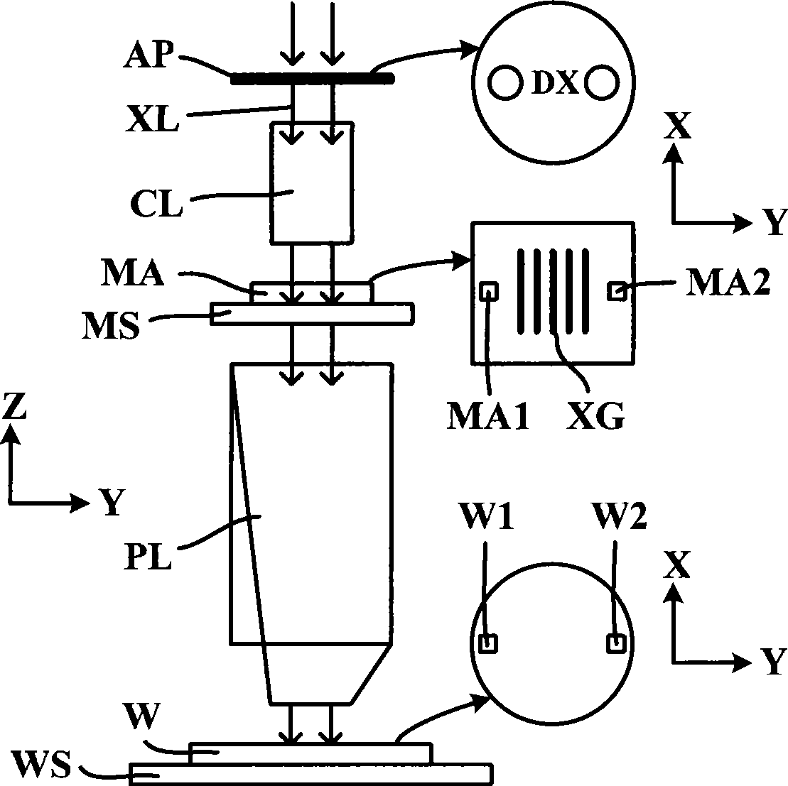
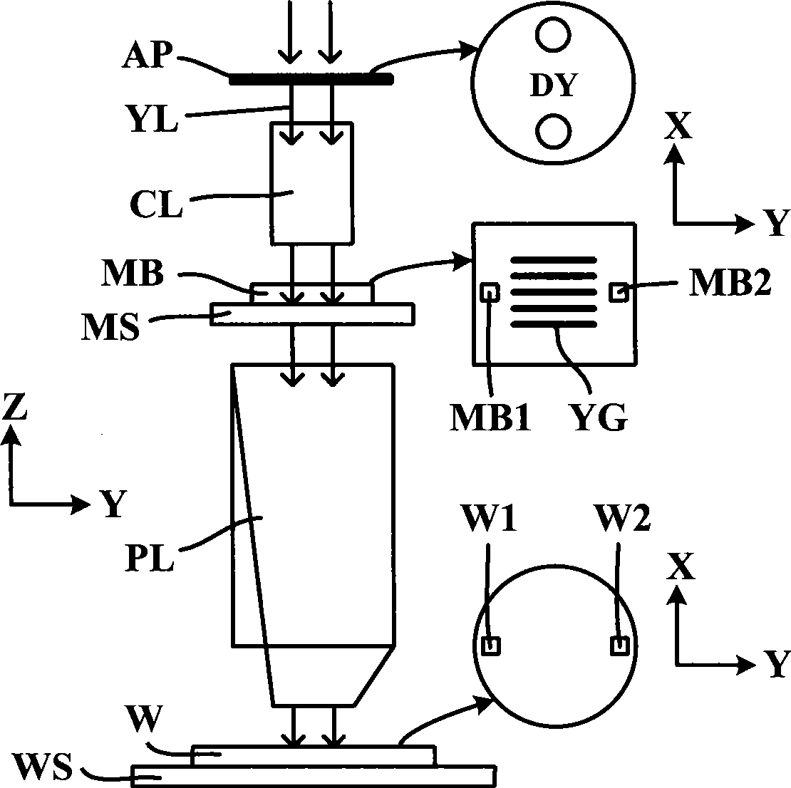
[0050] The exposure apparatus according to the embodiment of the present invention such as Figure 3A As shown, the exposure device includes: a light source system, an illumination system CL, a mask stage MS', a projection system PL, and a wafer stage WS.

[0051] The light source system generates the exposure light source. The light source system includes the aperture AP. Adjusting the position of the aperture APH of the aperture AP can make the exposure light source passing through the aperture AP form an X p...


PUM


Abstract

The invention relates to an exposure device and a method thereof. The exposure method comprises: positioning a first mask plate provided with a first direction layout pattern and a second mask plate provided with a second direction layout pattern on a mask table which has an area for supporting the first mask plate and the second mask plate; positioning a wafer to be exposed on a wafer table; aligning the first mask plate with the wafer to be exposed; exposing the wafer in the first direction; aligning the second mask plate with the wafer to be exposed; and exposing the wafer in the second direction. The exposure device and the method thereof save the steps of converting the mask plates and aligning the mask plates with the mask table, so as to shorten exposure time, and improve production efficiency and performance of products.

Description

technical field [0001] The invention relates to a photolithography process, in particular to an exposure device and method. Background technique [0002] Photolithography is an indispensable and important technology in the integrated circuit manufacturing process. The photolithography process generally includes the following steps: First, apply a photosensitive material such as photoresist on the surface of the wafer, and after the photosensitive material is dried, expose the circuit design pattern on the mask to the photosensitive material with a specific light source through an exposure device. Then, develop the photosensitive material with a developer, and use the developed pattern as a mask to perform etching and other processes, and finally complete the transfer of the mask pattern. [0003] As the size of devices in the integrated circuit manufacturing process becomes smaller and smaller, the requirements for the photolithography process are also higher and higher. A...

Claims


Application Information

Patent Timeline
IPC IPC(8): G03F7/20G03F9/00
Inventor 李承赫
Owner SEMICON MFG INT (SHANGHAI) CORP
Why Eureka
Try Eureka