Electronic element installing method

An electronic component installation and component technology, applied in the direction of electrical components, electrical components, etc., can solve problems such as the inability to align the optical path, the expansion of mechanical errors, and the increase in the manufacturing cost of the placement machine, so as to achieve low difficulty in data processing and reduce measurement The number of times, the effect of improving placement efficiency

Inactive Publication Date: 2015-12-30
NEODEN TECH CO LTD
View PDF3 Cites 6 Cited by
  • Summary
  • Abstract
  • Description
  • Claims
  • Application Information

AI Technical Summary

Problems solved by technology

However, pure image capture devices can only capture images, not light sources, and cannot be aligned with each other through the optical path. Therefore, the optical axis alignment is usually performed with an additional light source device, which will increase the manufacturing cost of the placement machine ; Or it is achieved by naked eye alignment, which leads to further expansion of mechanical errors

Method used


Image

  • Electronic element installing method
  • Electronic element installing method
  • Electronic element installing method

Examples


Embodiment Construction

[0034] The present invention will be further described in detail below in conjunction with the examples, the following examples are explanations of the present invention and the present invention is not limited to the following examples.

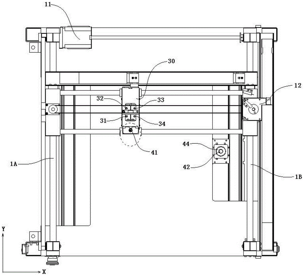
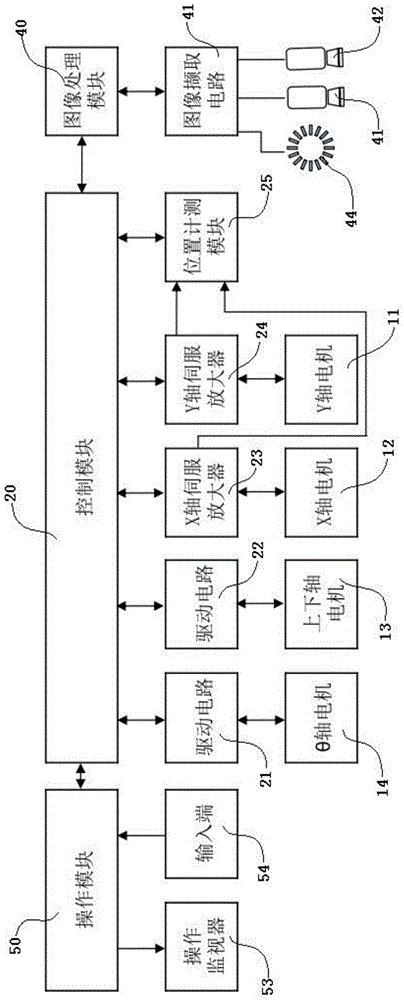
[0035] The desktop mounter is equipped with a conveying device for conveying printed circuit boards, a component supply device for supplying electronic components, a pair of arms 1A, 1B that can move in one direction (Y direction) by a Y-axis motor 11, and a pair of arms 1A, 1B that can be moved by an X-axis The motor 12 moves the placement head 30 along the two arms (X direction), and the X-Y coordinate system is the mechanical coordinate system of the placement head 30 .

[0036] Moreover, the suction nozzle 31 can be driven up and down by the vertical axis motor 13 via the drive circuit 22, and the suction nozzle 31 can be driven by the θ axis motor 14 via the drive circuit 21 to rotate around the vertical axis, so that the suction nozzle ...


PUM


Abstract

The invention relates to an electronic element installing method, in particular to an electronic element installing method which is applied to the field of desktop type chip mounters and comprises the steps that an image and recognition features of a suction nozzle are acquired through image capturing devices, and then an electronic element is installed on a printed circuit on the basis of a processing result of image information. According to the electronic element installing method, the rotating trace of the suction nozzle is acquired through a tracing mechanism, the step of optical axis alignment of the part and circuit board image capturing devices is omitted very skillfully, and the problem that the circuit board image capturing device cannot directly obtain the practical rotating center of the suction nozzle is solved; the relative position relation between the practical rotating center of the suction nozzle and an image capturing center of the circuit board image capturing device can be efficiently determined and deviation between the practical rotating center and a designed rotating center can be corrected on the basis that too much cost of an existing desktop type chip mounter structure is not increased, therefore, operating personnel can easily learn, and printed circuit board production chip mounting can be efficiently performed.

Description

technical field [0001] The present invention relates to a method for installing electronic components, in particular to a method applied in the field of desktop placement machines. The image of the suction nozzle and the identification features are acquired by an image capture device, and the electronic components are installed on the surface based on the processing results of the above image information. A method of mounting electronic components on a printed circuit. Background technique [0002] Mounting accuracy is one of the core performance requirements of placement machines. The suction nozzle of the desktop placement machine inevitably has mechanical errors during the assembly process, which leads to the inconsistency between the actual rotation center of the suction nozzle and the designed rotation center. The judgment deviation of position will ultimately affect the accuracy of electronic component installation. [0003] There are usually two image capture device...

Claims


Application Information

Patent Timeline
Patent Type & Authority Applications(China)
IPC IPC(8): H05K13/04H05K13/08
Inventor 翁建永施宝忠
Owner NEODEN TECH CO LTD
Why Eureka
Try Eureka