Shifting register and driving method thereof as well as gate drive circuit and display device

A technology for shift registers and gates, which is applied in the field of gate drive circuits, display devices, and shift registers, and can solve problems that affect the stable output of shift registers, large noises in scanning signals, and unstable gate potentials, etc.

Active Publication Date: 2015-12-02
BOE TECH GRP CO LTD +1
View PDF5 Cites 29 Cited by
  • Summary
  • Abstract
  • Description
  • Claims
  • Application Information

AI Technical Summary

Problems solved by technology

However, under the control of the clock signal, the shift register used in most GOA circuits at present, the node controlling the switching transistor for output will always be in a floating state, and the potential of this node will be affected by the leakage of the surrounding switching transistors, resulting in The gate potential of the switching transistor is unstable, which causes the scanning signal output by the drive signal output terminal to have relatively large noise, which in turn affects the stable output of the shift register.

Method used


Image

  • Shifting register and driving method thereof as well as gate drive circuit and display device
  • Shifting register and driving method thereof as well as gate drive circuit and display device
  • Shifting register and driving method thereof as well as gate drive circuit and display device

Examples


example 1

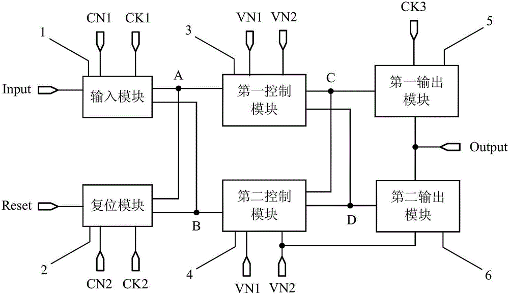
[0126] by Figure 2a The structure of the shift register shown is taken as an example to describe its working process, in which Figure 2aIn the shift register shown, all switching transistors are N-type switching transistors, each N-type switching transistor is turned on under the action of a high potential, and turned off under the action of a low potential; the potential of the first DC signal vn1 is a high potential, The potential of the second DC signal vn2 is a low potential; the potential of the first reference signal cn1 is a high potential, and the potential of the second reference signal cn2 is a low potential; the corresponding input and output timing diagram is as follows Figure 4a shown. Specifically, choose Figure 4a The input-output timing diagram shown has four stages: the input stage S1, the output stage S2, the reset stage S3 and the reset hold stage S4.

[0127] In the input stage S1, ck1=0, ck3=0, input=1, reset=0.

[0128] Since reset=0, the third sw...

example 2

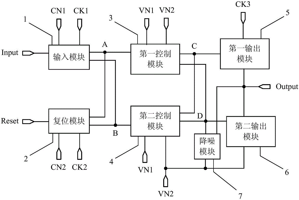
[0138] by Figure 3a The structure of the shift register shown is taken as an example to describe its working process, in which Figure 3a In the shift register shown, all switching transistors are N-type switching transistors, each N-type switching transistor is turned on under the action of a high potential, and turned off under the action of a low potential; the potential of the first DC signal vn1 is a high potential, The potential of the second DC signal vn2 is a low potential; the potential of the first reference signal cn1 is a high potential, and the potential of the second reference signal cn2 is a high potential; the corresponding input and output timing diagram is as follows Figure 4b shown. Specifically, choose Figure 4b The input-output timing diagram shown has four stages: the input stage S1, the output stage S2, the reset stage S3 and the reset hold stage S4.

[0139] In the four stages of the input stage S1, the output stage S2, the reset stage S3 and the ...


PUM


Abstract

The invention discloses a shifting register and a driving method thereof as well as a gate drive circuit and a display device. The shifting register comprises an input module, a reset module, a first control module, a second control module, a first output module and a second output module. According to the shifting register disclosed by the invention, through mutual cooperation of the six modules, the electric potential of a third node for controlling the first output module is at a stable state under the action of the first control module, and the electric potential of a fourth node for controlling the second output module is at a stable state under the action of the second control module, so that the stability of a scanning signal output from a driving signal output end of the shifting register is realized, the noise of the scanning signal output from the driving signal output end is further reduced, and the output stability of the shifting register is improved.

Description

technical field [0001] The invention relates to the field of display technology, in particular to a shift register, a driving method thereof, a gate driving circuit and a display device. Background technique [0002] With the rapid development of display technology, displays show a development trend of high integration and low cost. Among them, the GOA (GateDriveronArray, array substrate row drive) technology integrates the TFT (ThinFilmTransistor, thin film transistor) gate switch circuit on the array substrate of the display panel to form a scan drive for the display panel, which can save the gate integrated circuit ( IC, Integrated Circuit) bonding (Bonding) area and fan-out (Fan-out) area wiring space, not only can reduce product cost in terms of material cost and manufacturing process, but also can make the display panel symmetrical on both sides and narrow border In addition, this integration process can also save the Bonding process in the direction of the gate scann...

Claims


Application Information

Patent Timeline
Patent Type & Authority Applications(China)
IPC IPC(8): G09G3/20G11C19/28
CPCG09G3/20G09G3/3266G09G3/3677G09G2300/0408G09G2310/0267G09G2310/0286G09G2310/061G09G2320/0223G11C19/00G11C19/28
Inventor 王继国
Owner BOE TECH GRP CO LTD
Why Eureka
Try Eureka