A pure red optically variable anti-counterfeit pigment and preparation method thereof
A pigment and optical technology, applied in the field of pure red optical color-changing anti-counterfeiting pigments and its preparation, can solve problems such as color cast, inability to realize a single main reflection peak in a pure red area, and inability to display a pure red spectral color, etc., to achieve low production costs , rich color display effect, the effect of mature process conditions
- Summary
- Abstract
- Description
- Claims
- Application Information
AI Technical Summary
Problems solved by technology
Method used
Image
Examples
preparation example Construction
[0049] The present invention also provides a preparation method of pure red optically variable anti-counterfeiting pigment, comprising the following steps:
[0050] 1) Select a smooth and polished stainless steel substrate or glass substrate;
[0051] 2) Prepare an isolation film layer: apply the substrate obtained in step 1) to obtain an isolation film layer;
[0052] 3) Preparation of pure red optical color-changing film: the second semi-absorbing layer, the second dielectric layer, the first semi-absorbing layer, the first dielectric layer, and the second semi-absorbing film layer are sequentially coated on the isolation film layer obtained in step 2) , a central reflective layer, a first dielectric layer, a first semi-absorbing layer, a second dielectric layer, and a second semi-absorbent layer to obtain structural film layers symmetrically arranged on both sides of the central reflective layer;
[0053] 4) Prepare the isolation film layer and repeat the coating process o...
Embodiment 1
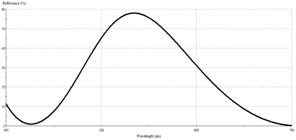
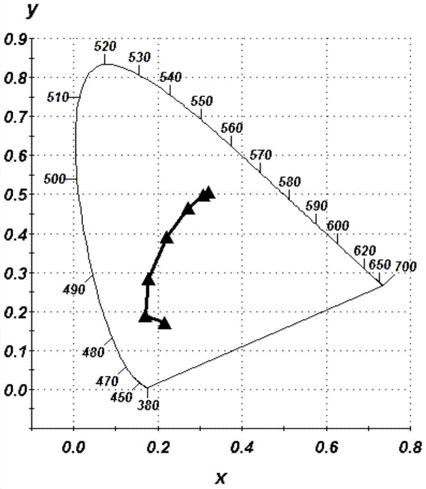
[0060] Figure 5 It is a schematic diagram of the structure of the pure red 9-layer metal medium symmetrical optically variable anti-counterfeiting film layer (pure red optically variable anti-counterfeiting pigment) of the present invention, and the film layer includes a second semi-absorbing layer 5, a second dielectric layer 4, a first Semi-absorbing layer 3, first dielectric layer 2, central reflective layer 1, first dielectric layer 2, first semi-absorbent layer 3, second dielectric layer 4, second semi-absorbent layer 5, said central reflective layer 1 is made of metal The material is made of titanium, and the thickness of the central reflection layer is 100nm. The second semi-absorbing layer 5 is used as a saturation adjustment layer and is made of a semi-absorbing metal thin film material Ti. The thickness of the second semi-absorbing layer is 3nm. The second dielectric layer 4 is used as a reflection sub-peak elimination film layer and is made of a transparent all-die...
Embodiment 2
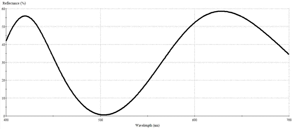
[0065] Figure 9 , is a schematic diagram of the structure of the pure red 7-layer metal medium symmetrical optically variable anti-counterfeiting film layer of the present invention, and the film layer includes a second dielectric layer 4, a first semi-absorbing layer 3, a first dielectric layer 2, and a central reflection layer in sequence. 1. The first dielectric layer 2, the first semi-absorbing layer 3, and the second dielectric layer 4. The central reflection layer 1 is made of metal material Al, and the thickness of the central reflection layer is 120 nm. Here, according to the different red regions required, the thickness of the second semi-absorbing layer 5 can be set to be 0, and the second dielectric layer 4 is used as a reflection sub-peak elimination film layer, which is made of a transparent all-dielectric material; the material of the second dielectric layer for MgF 2 , the thickness of the second dielectric layer 4 is 335nm; the first semi-absorbing layer 3 is...
PUM
| Property | Measurement | Unit |
|---|---|---|
| thickness | aaaaa | aaaaa |
| thickness | aaaaa | aaaaa |
| thickness | aaaaa | aaaaa |
Abstract
Description
Claims
Application Information
 - R&D
- Intellectual Property
- Life Sciences
- Materials
- Tech Scout
- Unparalleled Data Quality
- Higher Quality Content
- 60% Fewer Hallucinations
Browse by: Latest US Patents, China's latest patents, Technical Efficacy Thesaurus, Application Domain, Technology Topic, Popular Technical Reports.
© 2025 PatSnap. All rights reserved.Legal|Privacy policy|Modern Slavery Act Transparency Statement|Sitemap|About US| Contact US: help@patsnap.com


