Display base board and manufacturing method and display panel thereof

A display substrate and substrate substrate technology, applied in nonlinear optics, instruments, optics, etc., can solve problems such as damage to metal wires in the PAD area, and achieve the effects of simplifying the production process and reducing production costs

Inactive Publication Date: 2015-12-09
BOE TECH GRP CO LTD
View PDF8 Cites 14 Cited by
  • Summary
  • Abstract
  • Description
  • Claims
  • Application Information

AI Technical Summary

Problems solved by technology

[0006] Embodiments of the present invention provide a display substrate, a manufacturing method thereof, and a display panel, so as to sol

Method used


Image

  • Display base board and manufacturing method and display panel thereof
  • Display base board and manufacturing method and display panel thereof
  • Display base board and manufacturing method and display panel thereof

Examples


Embodiment Construction

[0043] Embodiments of the present invention provide a display substrate, a manufacturing method thereof, and a display panel to solve the problem in the prior art that metal wires in a PAD area are damaged when laser cutting technology is used to cut boxes.

[0044] The following will clearly and completely describe the technical solutions in the embodiments of the present invention with reference to the accompanying drawings in the embodiments of the present invention. Obviously, the described embodiments are only some, not all, embodiments of the present invention.

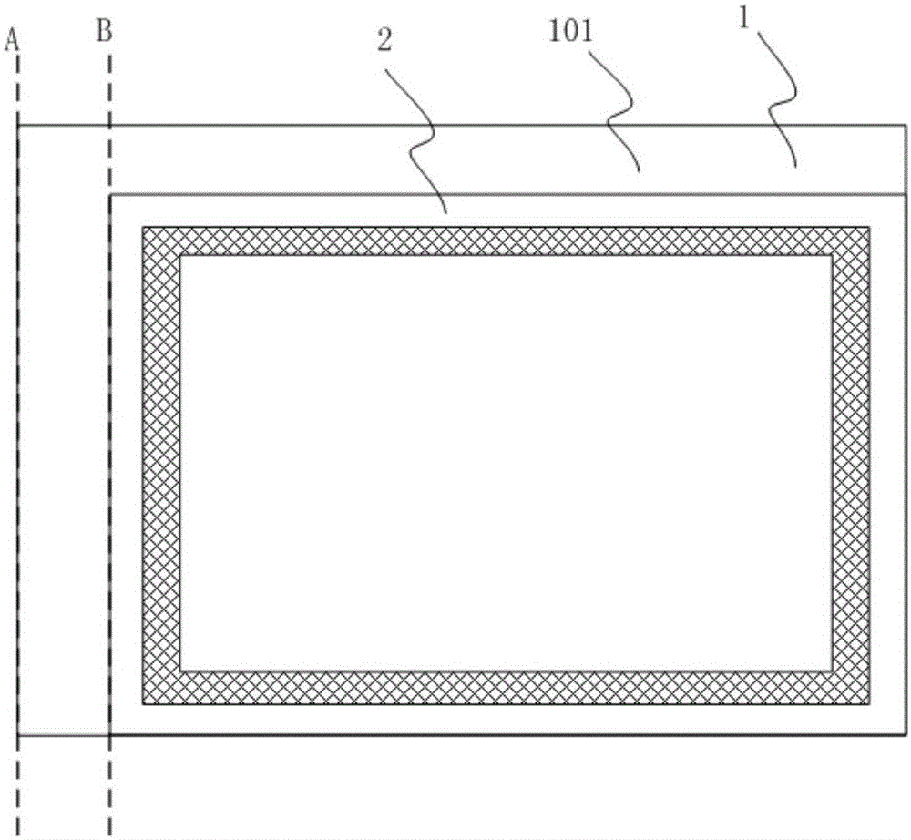
[0045] An embodiment of the present invention provides the display substrate, see Figure 4 ;from Figure 4 It can be seen from the figure that the display substrate includes a base substrate 41, a display area 42 and a PAD area 43 arranged on the base substrate 41, and the display substrate also includes at least a cutting line corresponding to the cutting line of the box substrate. The buffer layer 44 in the ...


PUM

PropertyMeasurementUnit
Thicknessaaaaaaaaaa

Abstract

The invention provides a display base board and a manufacturing method and display panel thereof and is used for solving the problem that in the prior art, metal wires in a PAD area are damaged when paired-box cutting is conducted by means of the laser cutting technology. The display base board comprises a substrate base board body, a display area and a PAD area, wherein the display area and the PAD area are arranged on the substrate base board body, the display base board further comprises a buffer layer which covers a cutting area corresponding to a cutting line of a paired-box base board at the minimum, and the buffer layer is used for preventing laser generated in the cutting process from damaging metal wires in the PAD area, wherein the cutting area is an area within a preset range at the two sides of a position, corresponding to the cutting line, of the display base board.

Description

technical field [0001] The invention relates to the technical field of liquid crystal display, in particular to a display substrate, a manufacturing method thereof, and a display panel. Background technique [0002] With the development of thin film transistor liquid crystal display technology and the progress of industrial technology, liquid crystal display technology has replaced cathode ray tube technology and become the mainstream technology in the field of daily display. Due to the reduction in production cost of liquid crystal display devices and the increasingly perfect manufacturing process, its own advantages have become ideal display devices in the minds of the market and consumers. At present, the stereoscopic display technology is rising day by day in the market, so it is also necessary to solve the technical shortcomings of the stereoscopic display technology and improve the imaging quality (such as reducing color cast, reducing bright spots, bright lines, reduc...

Claims


Application Information

Patent Timeline
IPC IPC(8): G02F1/1333
CPCG02F1/133351
Inventor 谭纪风陈立强
Owner BOE TECH GRP CO LTD
Why Eureka
Try Eureka