Varistor and its leads

A technology of piezoresistors and leads, which is applied in the direction of piezoresistors, resistors, resistor parts, etc., can solve the problems of small contact area between leads and soldered substrates, high current density of piezoresistors, and poor impact resistance. To reduce the thickness of the silver layer and the amount of the silver layer, increase the contact area, and enhance the impact resistance

Active Publication Date: 2019-08-16
CHENGDU TIEDA ELECTRONICS CORP
View PDF8 Cites 0 Cited by
  • Summary
  • Abstract
  • Description
  • Claims
  • Application Information

AI Technical Summary

Problems solved by technology

[0007] The purpose of the present invention is to overcome the lead wire structure of the existing piezoresistor so that the contact area between the wire and the welding substrate is small, resulting in low clamping reliability, and also causing the piezoresistor to fail when the piezoresistor impact test is performed. The current density is high, the impact resistance of the product is not strong, and at the same time, more silver layers need to be plated on the soldered substrate, and the overall cost of the product is relatively high. To provide a varistor and its leads, the varistor The contact area between the lead wire of the device and the welding substrate is large, which enhances the resistance to high current impact of the piezoresistor, and can also reduce the thickness of the silver layer on the welding substrate, greatly saving the overall production cost

Method used


Image

  • Varistor and its leads
  • Varistor and its leads
  • Varistor and its leads

Examples


Embodiment 1

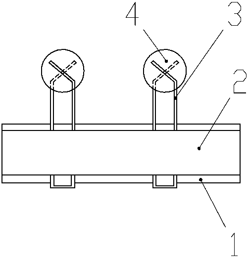
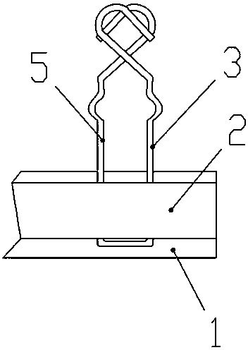
[0033] In this embodiment, the varistor lead whose free end is a U-shaped structure is applied to a 25KS varistor, such as Figure 2 to Figure 4 As shown, the varistor lead includes a first lead 3 and a second lead 5 that are bent into a symmetrical structure along the middle, and the first lead 3 and the second lead 5 include a straight line 31 close to the middle of the bend, Curved section 32 between the U-shaped section 33 of free end and straight section 31 and U-shaped section 33, described straight section 31 is used for fixing with paper tape 1 and adhesive tape 2, the U-shaped of first lead wire 3 and second lead wire 5 The section 33 is used to hold the solder substrate 4 .

[0034] In this example, if figure 2 and image 3 As shown, the lead wire of the present embodiment is a copper wire with a diameter of 1.2 mm, and the lead wire is flattened to 1.4 mm in width of the lead wire of the U-shaped section 33, so that the lead wire width of the U-shaped section 33 ...

Embodiment 2

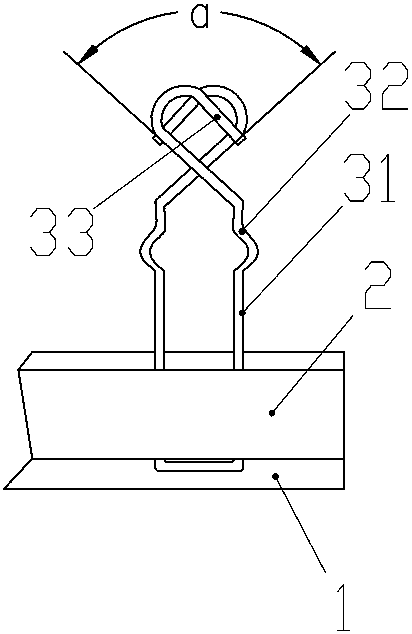
[0047] Such as Figure 2 to Figure 4 As shown, the varistor lead includes a first lead 3 and a second lead 5 that are bent into a symmetrical structure along the middle, and the first lead 3 and the second lead 5 include a straight line 31 close to the middle of the bend, Curved section 32 between the U-shaped section 33 of free end and straight section 31 and U-shaped section 33, described straight section 31 is used for fixing with paper tape 1 and adhesive tape 2, the U-shaped of first lead wire 3 and second lead wire 5 The section 33 is used to hold the solder substrate 4 .

[0048] In this embodiment, the included angle a of the U-shaped side of the U-shaped section 33 of the first lead 3 and the second lead 5 is 45° in this embodiment. The included angle of the U-shaped side of the U-shaped section of the first lead and the second lead determines the clamping position of the lead on the soldered substrate, and a is set to 45°, which can ensure that the clamping stabilit...

Embodiment 3

[0050] Such as Figure 2 to Figure 4 As shown, the varistor lead includes a first lead 3 and a second lead 5 that are bent into a symmetrical structure along the middle, and the first lead 3 and the second lead 5 include a straight line 31 close to the middle of the bend, Curved section 32 between the U-shaped section 33 of free end and straight section 31 and U-shaped section 33, described straight section 31 is used for fixing with paper tape 1 and adhesive tape 2, the U-shaped of first lead wire 3 and second lead wire 5 The section 33 is used to hold the solder substrate 4 .

[0051] In this embodiment, the included angle a of the U-shaped side of the U-shaped section 33 of the first lead 3 and the second lead 5 is 145° in this embodiment. The included angle of the U-shaped side of the U-shaped section of the first lead and the second lead determines the clamping position of the lead on the soldered substrate, and a is set to 145°, which can ensure that the clamping stabil...


PUM


Abstract

The invention discloses a resistor and particularly discloses a piezoresistor and a lead thereof. The piezoresistor lead comprises a first lead body and a second lead body which are bent to be of a symmetrical structure along the middle part. The first lead body and the second lead body both comprise linear sections close to the bent middle part, U-shaped sections located at the free ends and curved sections located between the linear sections and the U-shaped sections. The linear sections are used for fixing a paper tape and adhesive tape. The U-shaped section of the first lead body and the U-shaped section of the second lead body are used for clamping welding substrates. According to the structure of the lead of the piezoresistor, the free ends of the leads, used for clamping the welding substrates, are arranged to be of a U-shaped structure, the contact area of the lead and the welding substrates is doubled, and clamping reliability is improved. Meanwhile, the contact resistance is reduced along with the increase of the contact area; when an impulse test of the piezoresistor is carried out, the electric current density of the piezoresistor is reduced, and the impact resistance of products is enhanced; the quantity of silver layers needing to be plated on the welding substrates is reduced, and the production cost of the products is lowered.

Description

[0001] This case claims the priority of the Chinese utility model patent filed on July 31, 2015, with application number 201520567663.1. technical field [0002] The invention relates to a resistor, in particular to a piezoresistor and its lead. Background technique [0003] Both varistor and chip capacitor products in the prior art need to have electrodes drawn out. For example, the electrodes drawn out from varistors are welding leads. The general form is as follows: figure 1 As shown, one end of the lead wire 3 is arranged on the paper tape 1 and the adhesive tape 2, and the other end is used to clamp the welding substrate 4. The lead wire 3 is a copper wire folded in half along the middle, and the two free ends of the lead wire are placed on the welding substrate respectively. 4, the lead wire 3 is arranged in the form of an oblique straight line near the free end, so as to better contact and weld with the welding substrate; but there are still some problems in this stru...

Claims


Application Information

Patent Timeline
Patent Type & Authority Patents(China)
IPC IPC(8): H01C1/144H01C7/10
Inventor 张治成石小龙
Owner CHENGDU TIEDA ELECTRONICS CORP
Why Eureka
Try Eureka