Fabrication method of wafer level bump package structure

A technology of packaging structure and manufacturing method, which is applied in semiconductor/solid-state device manufacturing, electrical components, electric solid-state devices, etc., can solve problems such as no improvement in glue coating, increase in packaging costs, and limited improvement in product reliability. The effect of reducing chipping, improving reliability, and improving packaging reliability

Inactive Publication Date: 2015-12-09
NAT CENT FOR ADVANCED PACKAGING
View PDF5 Cites 9 Cited by
  • Summary
  • Abstract
  • Description
  • Claims
  • Application Information

AI Technical Summary

Problems solved by technology

[0004] The disadvantage of this method is that the replacement of the protective glue increases the packaging cost, and the degree of improvement of product reliability is limited; at the same time, the glue change does not improve the glue wrapping phenomenon during the cutting process.

Method used


Image

  • Fabrication method of wafer level bump package structure
  • Fabrication method of wafer level bump package structure
  • Fabrication method of wafer level bump package structure

Examples


Embodiment Construction

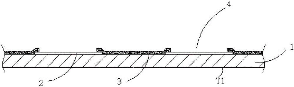
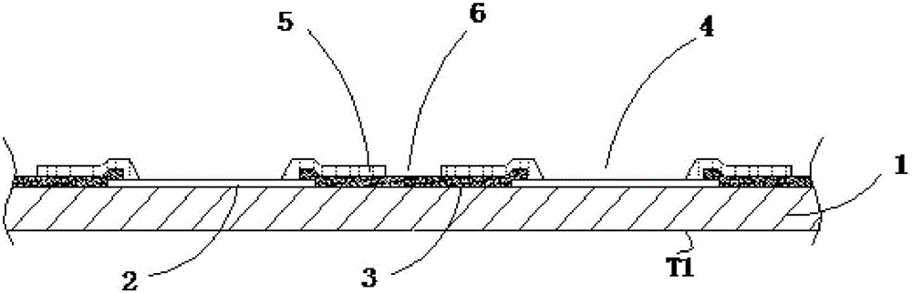
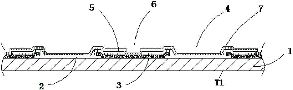
[0039] In order to make the above objects, features and advantages of the present invention more comprehensible, the specific implementation manners of the present invention will be further described below in conjunction with specific drawings.

[0040] In the following description, a lot of specific details are set forth in order to fully understand the present invention, but the present invention can also be implemented in other ways that are different from those described here, and those skilled in the art can do so without departing from the connotation of the present invention. By analogy, the present invention is not limited by the specific examples disclosed below.

[0041] Secondly, the present invention is described in detail in combination with schematic diagrams. When describing the embodiments of the present invention in detail, for the convenience of explanation, the cross-sectional view showing the device structure will not be partially enlarged according to the g...


PUM


Abstract

The invention relates to a fabrication method of a wafer level bump package structure. The method comprises the following steps: (1) providing a wafer integrated with a chip electrode and an insulating layer; (2) fabricating a protective layer on the wafer; (3) removing the protective layer above the chip electrode to form a first opening, and removing the protective layer at a chip cutting position on the wafer to form a second opening; (4) fabricating an under bump metal layer and a bump layer at the first opening; and (5) carrying out cutting along the position of the second opening to obtain a single wafer level bump package structure. According to the fabrication method, the problem of overlarge stress, for pulling the insulating layer, of the protective layer due to thermal mismatching is avoided, so that the package reliability is improved; and when the reliability is improved, the processing step is not increased. In the wafer cutting process, protection glue at the preset cutting position is removed, so that the protective layer avoids a cutting channel; pulling of the insulating layer by the protective layer during cutting is removed; and the edge breakage phenomenon of a chip body during cutting is reduced.

Description

technical field [0001] The invention relates to a method for manufacturing a wafer-level bump packaging structure, which belongs to the technical field of semiconductor packaging. Background technique [0002] During the cutting of the wafer-level bump package structure and the reliability test of the bump package, cracking of the insulating layer occurs during the process and test. [0003] In the existing technology, to solve this technical problem, companies generally replace the protective glue to reduce the thermal mismatch between the protective glue, insulating layer and silicon, thereby reducing the pull of the protective glue on the insulating layer, thereby reducing the need for packaging reliability testing. The failure phenomenon that occurs in the bump package structure. [0004] The disadvantage of this method is that the replacement of the protective glue increases the packaging cost, and the improvement of product reliability is limited by the replacement of...

Claims


Application Information

Patent Timeline
Patent Type & Authority Applications(China)
IPC IPC(8): H01L23/485H01L21/60H01L21/78
CPCH01L2224/11
Inventor 曹立强何洪文戴风伟秦飞史戈别晓锐
Owner NAT CENT FOR ADVANCED PACKAGING
Why Eureka
Try Eureka