
Multisystem signal simulation device and method

A signal simulation, multi-standard technology, used in baseband system components, shaping networks in transmitters/receivers, etc., can solve the problems of complex signal conditioning circuit design, poor signal flatness, and inability to cover frequency bands, and achieve simplification FPGA internal design, reduced performance requirements, high consistency

Active Publication Date: 2015-12-09
THE 41ST INST OF CHINA ELECTRONICS TECH GRP
View PDF4 Cites 30 Cited by
  • Summary
  • Abstract
  • Description
  • Claims
  • Application Information

AI Technical Summary

Problems solved by technology

[0011] Existing signal simulators have few signal styles, and the frequency band cannot cover shortwave, ultrashort wave, and satellite communication frequency bands. The internal digital domain of FPGA directly completes the design of carrier modulation signal, and the signal carrier frequency and modulation signal frequency are affected by the maximum clock rate of FPGA. To generate higher-frequency data streams requires careful design of data interpolation and combination processing and filtering processing, which is difficult to design; at the same time, the requirements for DAC sampling rate and data bit width are high, and multiple frequency conversion processing is required to cover a wider frequency range , making the design of the signal conditioning circuit complex, with more spurious signals and poor flatness of uncompensated signals

Method used


Image

  • Multisystem signal simulation device and method
  • Multisystem signal simulation device and method
  • Multisystem signal simulation device and method

Examples


Embodiment Construction

[0047]The following will clearly and completely describe the technical solutions in the embodiments of the present invention with reference to the accompanying drawings in the embodiments of the present invention. Obviously, the described embodiments are only some, not all, embodiments of the present invention. Based on the embodiments of the present invention, all other embodiments obtained by persons of ordinary skill in the art without making creative efforts belong to the protection scope of the present invention.

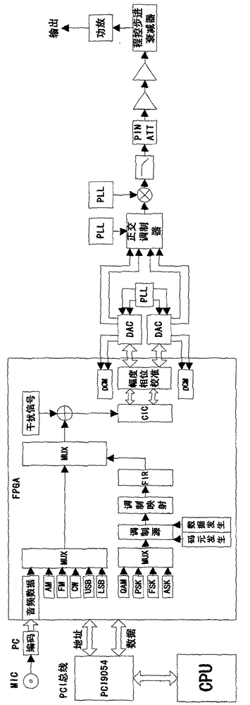
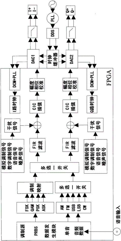
[0048] When the multi-system signal simulation device of the present invention is working, the host computer first selects the modulation type, and then sets the relevant parameters of the modulation type, such as the modulation frequency of the amplitude modulation signal, the depth of amplitude modulation, etc.; the relevant parameters are calculated and calculated in the FPGA. Conversion, through digital signal processing, output 16-bit data stream, realize b...


PUM


Abstract

The invention provides a multisystem signal simulation device comprising a baseband signal generation module and a signal conditioning module. The baseband signal generation module comprises two parts of a digital circuit and an analog circuit. The analog circuit part comprises an analog clock circuit and a digital-to-analog conversion circuit. The digital circuit part comprises a clock management module, a data generation module, a digital modulation module, an FIR formation filtering module, a CIC interpolation module and an amplitude and phase calibration module. The signal conditioning module comprises an orthogonal modulation module, a broadband frequency conversion module, an amplitude control module and an amplification attenuation module. A baseband orthogonal modulation signal is realized in the internal part of an FPGA so that degree of complexity of the baseband signal design in the FPGA can be reduced, the requirement for DAC sampling rate and data width can be reduced and high-index output of a carrier modulation signal can be realized. A radio frequency PIN amplitude control technology is adopted so that small step and high dynamic range of signal amplitude can be realized.

Description

technical field [0001] The invention relates to the field of signal generation, in particular to a multi-standard signal simulation device, and also relates to a multi-standard signal simulation method. Background technique [0002] The multi-standard signal simulation device is a multi-purpose signal excitation source, including analog signals such as Morse newspaper signal, voice report signal, AM signal, FM signal, single sideband signal, and QAM, PSK, FSK, ASK, etc. Standard signals such as digital standard signals, noise signals, and interference signals. [0003] With the development of electronic technology, multi-standard signal simulation devices have been widely used in various fields such as wireless communication, radar, electronic countermeasures, and satellite communications. They are mainly used in simulating various complex communication environments and communication countermeasure environments. Manufacturers of countermeasure equipment provide comprehensiv...

Claims


Application Information

Patent Timeline
IPC IPC(8): H04L25/03
Inventor 朱勇锋陈应兵
Owner THE 41ST INST OF CHINA ELECTRONICS TECH GRP
Learn More