A mems structure and manufacturing method thereof

A production method and technology for bonding materials, which are applied in microstructure technology, microstructure devices, manufacturing microstructure devices, etc., can solve problems such as very high process capability requirements, affecting product yield, etc., and achieve low process capability requirements and finished products. The effect of high rate and reliable fixing method

Active Publication Date: 2016-12-07
无锡微文半导体科技有限公司
View PDF9 Cites 0 Cited by
  • Summary
  • Abstract
  • Description
  • Claims
  • Application Information

AI Technical Summary

Problems solved by technology

The disadvantage is that the process capability is very high. If there is a slight deviation in the bonding alignment during the bonding process, it will affect the yield of the entire product.

Method used


Image

  • A mems structure and manufacturing method thereof
  • A mems structure and manufacturing method thereof
  • A mems structure and manufacturing method thereof

Examples


Embodiment 1

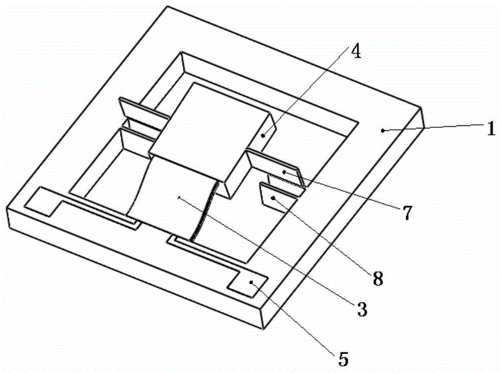
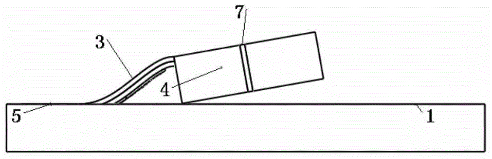
[0048] Such as figure 1 As shown, a MEMS structure includes a substrate 1, a suspended component 4, such as a mass or a mirror, and a controllable deformation component 3, wherein one end of the controllable deformation component 3 is connected to the substrate 1 , the other end is connected to the suspended component 4; a first connecting portion 7 is provided on the side of the suspended component 4; one end of the first connecting portion 7 is fixedly connected to the suspended component 4, and the other end is suspended. A second connection part 8 is provided on the substrate 1, and the second connection part 8 forms a matching relationship with the first connection part 7; the application of this structure can be applied to fields such as micro-optical light path adjustment and optical communication.

[0049] The substrate 1 provides a support for the MEMS structure of the present invention;

[0050] The first connecting portion 7 and the second connecting portion 8 are us...

Embodiment 2

[0070] The main difference between this embodiment and embodiment 1 is that the symmetrically distributed controllable deformation component 3 is used; the controllable deformation component 3 is made of Cu and W materials with different expansion coefficients;

[0071] Such as Figure 10 As shown, a MEMS structure includes a substrate 1, a suspended component 4 (such as a mass or a mirror), two symmetrically distributed controllable deformation components 3, one end of the controllable deformation component 3 is connected to the The substrate 1 is connected, and the other end is connected to the suspended component 4; a first connecting portion 7 is provided on the side of the suspended component 4; one end of the first connecting portion 7 is fixedly connected to the suspended component 4, and the other end dangling. A second connection part 8 is provided on the substrate 1, and the second connection part 8 forms a matching relationship with the first connection part 7; the...

Embodiment 3

[0089] The main difference between this embodiment and embodiment 1 is that the controllable deformation part 3 is made of Au, SiO 2 Two kinds of materials with different expansion coefficients are compounded, and its effect is to lift the suspended part 4 above the surface of the substrate 1; and there is no electric lead 5; what the bonding material 6 uses is epoxy resin glue.

[0090] Such as Figure 9 As shown, a MEMS structure includes a substrate, a suspended part (mass or mirror), and a single controllable deformation part, wherein one end of the controllable deformation part is connected to the substrate, and the other end is connected to the suspended part. The suspension part is connected; a first connection part 7 is provided on the side of the suspended part; one end of the first connection part 7 is fixedly connected with the suspended part, and the other end is suspended. The application of the structure can be applied to the fields of micro-optical light path a...


PUM


Abstract

A MEMS structure comprises a substrate (1), a controllable deformation part (3), and a suspended part (4) connected with the substrate (1) through at least one controllable deformation part (3), and further comprises a first connecting part (7) located on the suspended part (4) and a second connecting part (8) located on the substrate (1). A method for fabricating a MEMS structure is provided, wherein the controllable deformation part (3) is a structure formed by stacking at least two materials having different expansion coefficients. Deformation of the controllable deformation part (3) is controlled by externally heating or cooling the entire MEMS structure, thereby changing a suspension height or angle of the suspended part (4). When the suspension height or angle of the suspended part (4) meets a set requirement, the first connecting part (7) on the suspended part (4) and the second connecting part (8) on the substrate (1) are connected and fixed by an adhesive material (6). The method achieves a precise, accurate and reliable fixed connection in the MEMS structure.

Description

technical field [0001] The invention belongs to the field of micromechanical systems (MEMS), and relates to a MEMS structure and a manufacturing method thereof. Background technique [0002] The development of micro-electromechanical systems (MEMS) technology has opened up a new technical field and industry. Micro-sensors, micro-actuators, micro-components, micro-mechanical optical devices, vacuum microelectronic devices, power electronic devices, etc. made by MEMS technology are used in aviation , Aerospace, automobile, biomedicine, environmental monitoring, military and almost all fields that people come into contact with have very broad application prospects. [0003] The controllable deformation component mentioned in the present invention may be a Bimorph structure. This structure has been applied to many fields. The article "Development and applications of high fill-factor, small footprintmems micromirrors and micromirror arrays" (the article is the doctoral dissertat...

Claims


Application Information

Patent Timeline
Patent Type & Authority Patents(China)
IPC IPC(8): B81B3/00B81C1/00
CPCB81B3/00B81C1/00
Inventor 程进陈巧丁金玲徐乃涛孙其梁谢会开
Owner 无锡微文半导体科技有限公司
Why Eureka
Try Eureka