

Display panel and manufacture method thereof
A technology of display panel and manufacturing method, applied in chemical instruments and methods, optics, instruments, etc., can solve the problem of high driving voltage
- Summary
- Abstract
- Description
- Claims
- Application Information
AI Technical Summary
Problems solved by technology
Method used
Image

Examples
Embodiment Construction
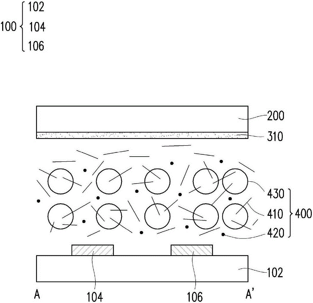
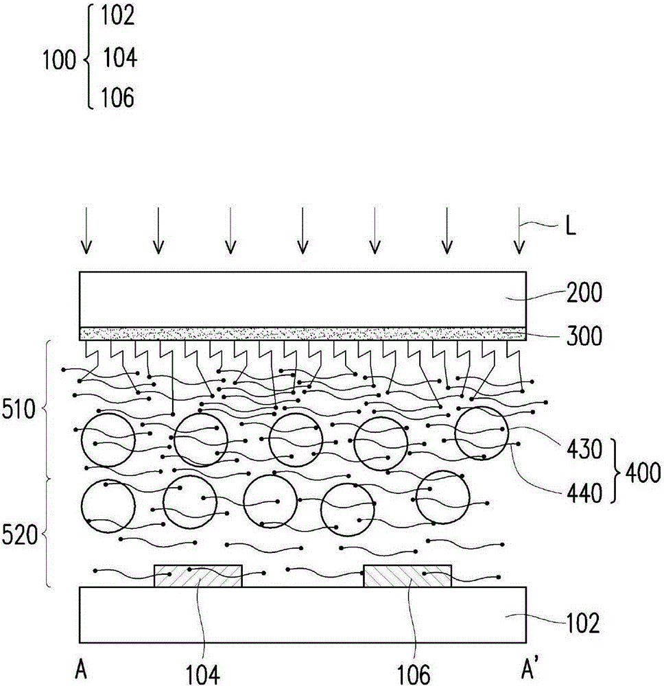
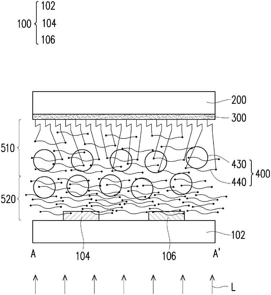
[0027] Figure 4 It is a schematic partial circuit diagram of a pixel array of a display panel according to an embodiment of the present invention. figure 1 is a partial cross-sectional view of the display panel before the lighting process according to an embodiment of the present invention, which corresponds to Figure 4 Sectional view of AA' in . figure 2 is a partial cross-sectional view of a display panel according to an embodiment of the present invention after an illumination procedure, along Figure 4 Sectional view of AA' in the middle.
[0028] Please refer to figure 1 , the display panel includes a pixel array substrate 100, an opposite substrate 200, and a liquid crystal material composition 400, wherein the pixel array substrate 100 includes a first substrate 102 and a pixel array (not shown) disposed on the first substrate 102, as Figure 4 shown. Figure 4 Only one of the data lines DL, one of the scan lines SL, one of the common electrode lines CL and one ...
PUM
 Abstract
Description
Claims
Application Information