Liquid crystal display panel and liquid crystal display panel ESD monitoring method
A liquid crystal display panel and display area technology, applied in nonlinear optics, instruments, optics, etc., can solve problems such as cost increase, production capacity decline, and impact on the quality of liquid crystal display panel products, and achieve the effect of predicting risks and improving products.
- Summary
- Abstract
- Description
- Claims
- Application Information
AI Technical Summary
Problems solved by technology
Method used
Image
Examples
Embodiment Construction
[0028] In order to further illustrate the technical means adopted by the present invention and its effects, the following describes in detail in conjunction with preferred embodiments of the present invention and accompanying drawings.
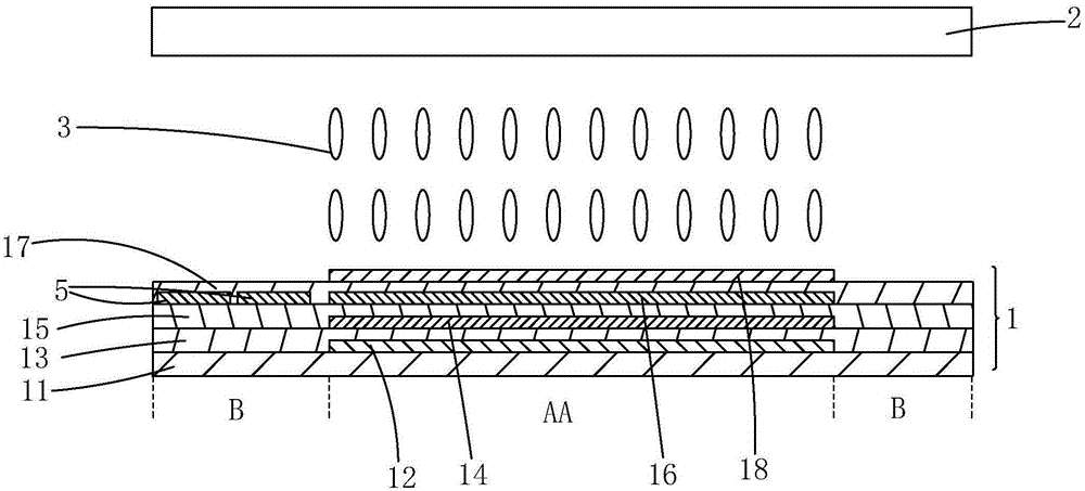
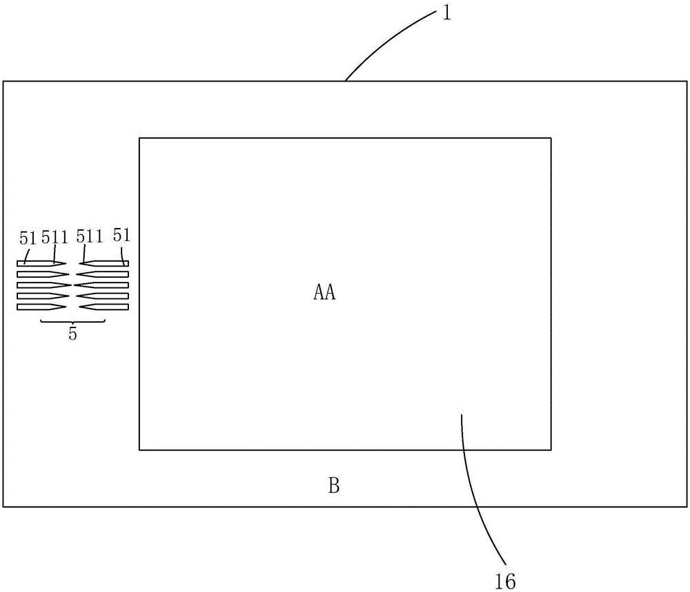
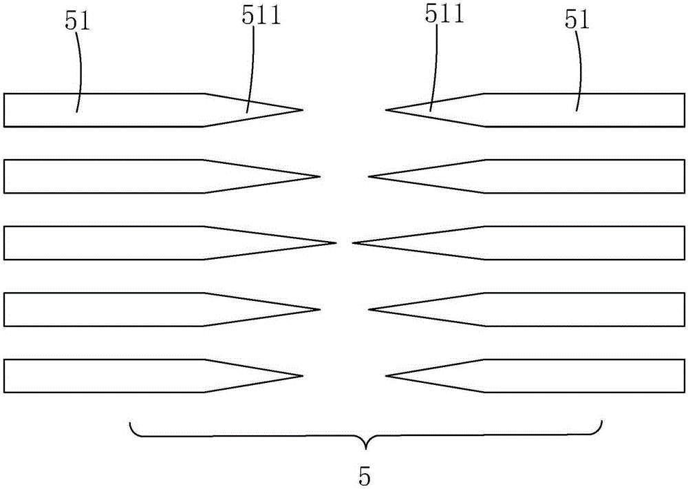
[0029] Please also see figure 1 , figure 2 ,and image 3 Firstly, the present invention provides a structure of a liquid crystal display panel, including: a TFT array substrate 1 , a CF substrate 2 , and a liquid crystal layer 3 arranged between the TFT array substrate 1 and the CF substrate 2 .
[0030] The TFT array substrate 1 has a display area AA and a peripheral area B without wires located on the periphery of the display area AA. The non-wired peripheral area B of the TFT array substrate 1 is provided with multiple groups of electrostatic discharge test elements 5 spaced from each other and arranged in parallel along the first direction, and each group of electrostatic discharge test elements 5 includes two In the second direction o...
PUM
 Abstract
Description
Claims
Application Information


