Shifting register, grid electrode integrated driving circuit and display device

A shift register, gate technology, applied in static memory, digital memory information, instruments, etc., can solve problems such as easy failure of shift registers

Active Publication Date: 2015-12-23
BOE TECH GRP CO LTD
View PDF6 Cites 67 Cited by
  • Summary
  • Abstract
  • Description
  • Claims
  • Application Information

AI Technical Summary

Problems solved by technology

[0005] In view of this, an embodiment of the present invention provides a shift register, a gate driving circuit and a display device to solve the problem that the existing shift register is prone to failure when working for a long time

Method used


Image

  • Shifting register, grid electrode integrated driving circuit and display device
  • Shifting register, grid electrode integrated driving circuit and display device
  • Shifting register, grid electrode integrated driving circuit and display device

Examples


Embodiment 1

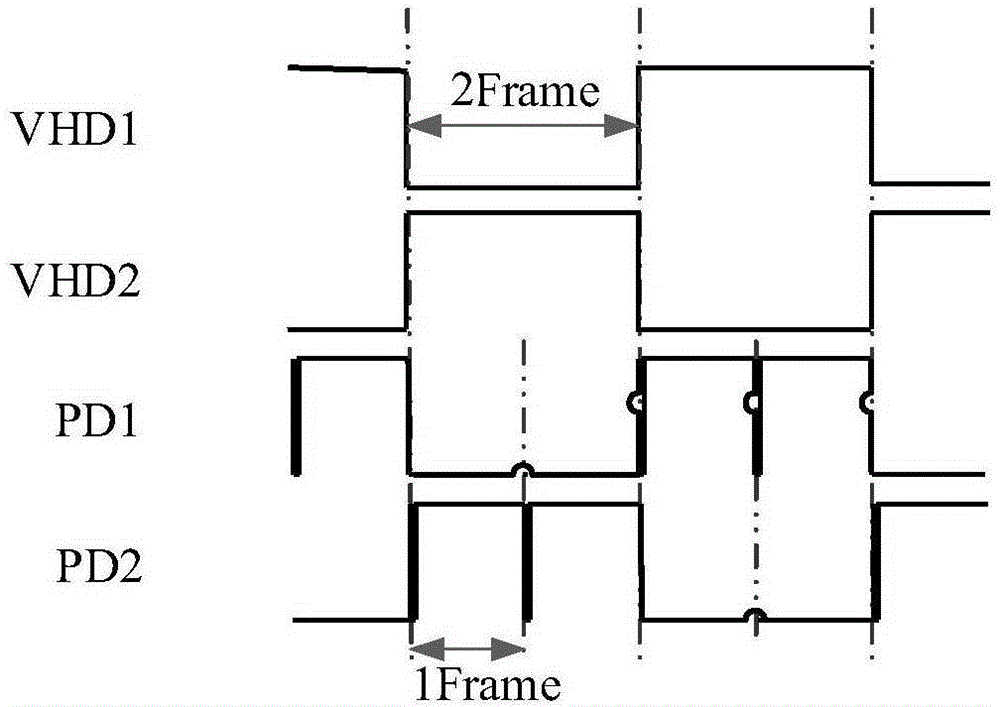
[0130] The first reset control signal terminal Rst1 and the second reset control signal terminal Rst2 are the same signal terminal, the first node control signal terminal VHD1 and the second node control signal terminal VHD2 alternately input the frequency of the node control signal and the clock signal terminal CLK input clock signal The frequency is the same, the corresponding input and output timing diagram is as follows Figure 5a shown. Specifically, choose the Figure 5a The four stages of T1, T2, T3 and T4 in the shown input and output timing diagram.

[0131] In the first phase T1, Input=1, Rst1=Rst2=0, CLK=0, VHD1=0, VHD2=1.

[0132] In the T1 stage, since Rst1 and Rst2 are at low potential, the second switch transistor T2 and the twentieth switch transistor T20 are turned off; because Input is at a high potential, the first switch transistor T1 is turned on, and the input signal is transmitted to the The first node PU, the potential of the first node PU is a high ...

Embodiment 2

[0141] The first reset control signal of the first reset control signal terminal Rst1 is delayed by 0.5 pulse width than the second reset control signal of the second reset control signal terminal Rst2, and the first node control signal terminal VHD1 and the second node control signal terminal VHD2 are alternately input The frequency of the node control signal is the same as the frequency of the input clock signal at the clock signal terminal CLK, and the corresponding input and output timing diagram is as follows Figure 5b shown. Specifically, choose the Figure 5b The four stages of T1, T2, T3 and T4 in the shown input and output timing diagram.

[0142] In the first phase T1, Input=1, Rst1=Rst2=0, CLK=0, VHD1=0, VHD2=1.

[0143] In the T1 stage, since Rst1 and Rst2 are at low potential, the second switch transistor T2 and the twentieth switch transistor T20 are turned off; because Input is at a high potential, the sixteenth switch transistor T16 to the nineteenth switch ...


PUM


Abstract

The invention relates to a shifting register, a grid electrode integrated driving circuit and a display device. The shifting register comprises an input module, a first resetting module, an output module, a first pulling-down control module and a second pulling-down control module, wherein the input module is used for controlling a potential of a first node to be a first potential; the output module is used for providing a clock signal at a clock signal end to a signal output end; the first resetting module is used for providing a reference signal of a reference signal end to the first node; a first node control signal end and a second node control signal end are used for alternatively inputting a node control signal, so that the first pulling-down control module and the second pulling-down control module work alternatively and a reference signal of the reference signal end is provided for the first node and the signal output end respectively; and the duty ratio of bias voltage of each pulling-down control module is reduced so that the working life of the shifting register is prolonged.

Description

technical field [0001] The invention relates to the field of display technology, in particular to a shift register, a gate integrated drive circuit and a display device. Background technique [0002] In today's era of rapid technological development, liquid crystal displays have been widely used in electronic display products, such as televisions, computers, mobile phones and personal digital assistants. The liquid crystal display includes a data driver (SourceDriver), a gate driver (GateDriver), and a liquid crystal display panel. The liquid crystal display panel has a pixel array, and the gate driving device is used to sequentially turn on the corresponding pixel rows in the pixel array, so as to transmit the pixel data output by the data driver to the pixels, and then display the image to be displayed. [0003] At present, the gate drive device is generally formed on the array substrate of the liquid crystal display through an array process, that is, the GateDriveronArra...

Claims


Application Information

Patent Timeline
Patent Type & Authority Applications(China)
IPC IPC(8): G09G3/36G11C19/28
CPCG09G3/2092G09G3/3266G09G3/3677G09G2310/0286G09G2310/0289G09G2310/08G11C19/28
Inventor 商广良韩承佑金志河韩明夫姚星郑皓亮林允植李承珉邱海军田正牧董学
Owner BOE TECH GRP CO LTD
Why Eureka
Try Eureka