Junction termination structure of transverse high-voltage power device

A power device, lateral high voltage technology, applied in the direction of semiconductor devices, electrical components, circuits, etc., can solve the problems of electric field curvature effect and charge imbalance at the connection, and optimize the breakdown voltage and charge imbalance. Improve and alleviate the problem The effect of the curvature effect

Active Publication Date: 2015-12-30
UNIV OF ELECTRONICS SCI & TECH OF CHINA
View PDF5 Cites 4 Cited by
  • Summary
  • Abstract
  • Description
  • Claims
  • Application Information

AI Technical Summary

Problems solved by technology

[0004] What the present invention aims to solve is to propose a junction terminal structure of a lateral high-voltage power device in view of the defects of the traditional device charge imbalance and the curvature effect of the electric field at the connection

Method used


Image

  • Junction termination structure of transverse high-voltage power device
  • Junction termination structure of transverse high-voltage power device
  • Junction termination structure of transverse high-voltage power device

Examples


Embodiment 1

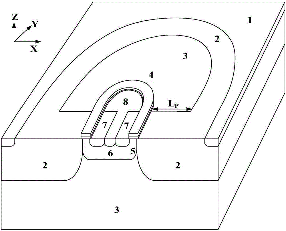
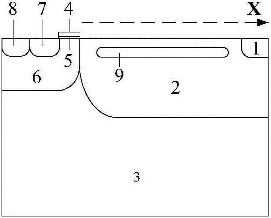
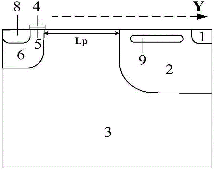
[0037] Such as Figure 5 As shown, the structure of this example includes a linear knot terminal structure and a curvature knot terminal structure;

[0038] The linear junction terminal structure is the same as that of the active region of the lateral high-voltage power device, including the drain N + Contact region 1, N-type drift region 2, P-type substrate 3, gate polysilicon 4, gate oxide layer 5, P-well region 6, source N + Contact area 7, source P + Contact region 8, P-type buried layer 9; P-well region 6 and N-type drift region 2 are located on the upper layer of P-type substrate 3, wherein P-well region 6 is located in the middle, with N-type drift region 2 on both sides, and P- The well region 6 is connected to the N-type drift region 2; the two sides of the N-type drift region 2 away from the P-well region 6 are the drain N + The surface of the contact region 1, the P-well region 6 has a source N connected to the metallized source + contact area 7 and the source P...

Embodiment 2

[0043] Such as Image 6 As shown, the difference between this example and Example 1 is that in this example, the junction of the P-type buried layer 9 in the linear junction termination structure and the P-type buried layer 9 in the curvature junction termination structure is located in the N-type drift region 2. The principle Same as Example 1.

Embodiment 3

[0045] Such as Figure 7 As shown, the difference between this example and Embodiment 1 is that the inner wall of the P-type buried layer 9 in the direct junction termination structure coincides with the inner wall of the N-type drift region 2 in the direct junction termination structure, and the P-type buried layer 9 in the curvature junction termination structure The inner wall is located in the P-type substrate 3, and the inner wall of the P-type buried layer 9 in the curvature junction terminal structure extends to the middle to connect with the inner wall of the P-type buried layer 9 in the direct junction termination structure. A circle, then a straight line with a distance of e, and finally a circular arc with a counterclockwise radius of one-twelfth of r1 to connect with the inner wall of the P-type buried layer 9 in the direct junction terminal structure; in the curvature junction terminal structure The distance between the inner wall of the ring-shaped P-type buried ...


PUM


Abstract

The invention belongs to the semiconductor technical field and relates to a junction termination structure of a transverse high-voltage power device. According to the structure of the invention, the inner wall of an N-type drift region 2 and the inner wall of a P type buried layer 9 in a curvature junction termination structure respectively extend to the middle so as to be connected with the inner wall of an N-type drift region 2 and the inner wall of a P type buried layer 9 in a direct junction termination structure, an extending route being a circular arc-shaped path; and therefore, curvature effects of electric fields at joints can be effectively alleviated; in a direction vertical to the extension direction of the joints, the P-type buried layers 9 exceed the N-type drift regions 2 by a certain distance, and therefore, the problem of charge imbalance can be solved. With the junction termination structure of the transverse high-voltage power device of the invention adopted, the problem of charge imbalance of the joints of the direct junction termination structure and the curvature junction termination structure and the problem of the curvature effects of the electric fields at the joints of the direct junction termination structure and the curvature junction termination structure can be solved, and pre-breakdown of the device can be avoided, and optimized breakdown voltage can be obtained.

Description

technical field [0001] The invention belongs to the technical field of semiconductors, and in particular relates to a junction terminal structure of a lateral high-voltage power device. Background technique [0002] The development of high-voltage power integrated circuits is inseparable from the integration of lateral high-voltage power semiconductor devices. Lateral high-voltage power semiconductor devices are usually closed structures, including circular, racetrack and interdigitated structures. For the closed racetrack structure and the interdigitated structure, there will be small curvature terminations in the curved part and the fingertip part, and the electric field lines are easy to concentrate at the small curvature radius, which will lead to early avalanche breakdown of the device at the small curvature radius , which poses new challenges to the layout structure of lateral high-voltage power devices. [0003] The Chinese patent with the publication number CN10224...

Claims


Application Information

Patent Timeline
Patent Type & Authority Applications(China)
IPC IPC(8): H01L29/06
CPCH01L29/0634
Inventor 乔明代刚张晓菲王裕如方冬张波
Owner UNIV OF ELECTRONICS SCI & TECH OF CHINA
Why Eureka
Try Eureka