GOA unit circuit and GOA circuit

A unit circuit and circuit node technology, applied in nonlinear optics, instruments, optics, etc., can solve the problems of unfavorable display frame narrowing design, output misalignment, etc.

Active Publication Date: 2016-01-06
TRULY HUIZHOU SMART DISPLAY
View PDF5 Cites 20 Cited by
  • Summary
  • Abstract
  • Description
  • Claims
  • Application Information

AI Technical Summary

Problems solved by technology

Each circuit part contains its own thin film transistor and capacitor. Therefore, the overall GOA unit circuit and cascaded GOA circuit include more thin film transistors and capacitors, and the GOA circuit is usually designed to be arranged on the edge of the pixel circuit. Therefore, it is not conducive to the narrow border design of the display
At the same time, the two circuit parts are independent of each other, and the problem of output misalignment is easy to occur.

Method used


Image

  • GOA unit circuit and GOA circuit
  • GOA unit circuit and GOA circuit
  • GOA unit circuit and GOA circuit

Examples


Embodiment Construction

[0036] In order to make the object, technical solution and advantages of the present invention clearer, the present invention will be further described in detail below in conjunction with the accompanying drawings and embodiments. It should be understood that the specific embodiments described here are only used to explain the present invention, not to limit the present invention.

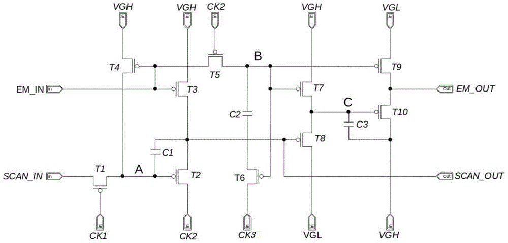
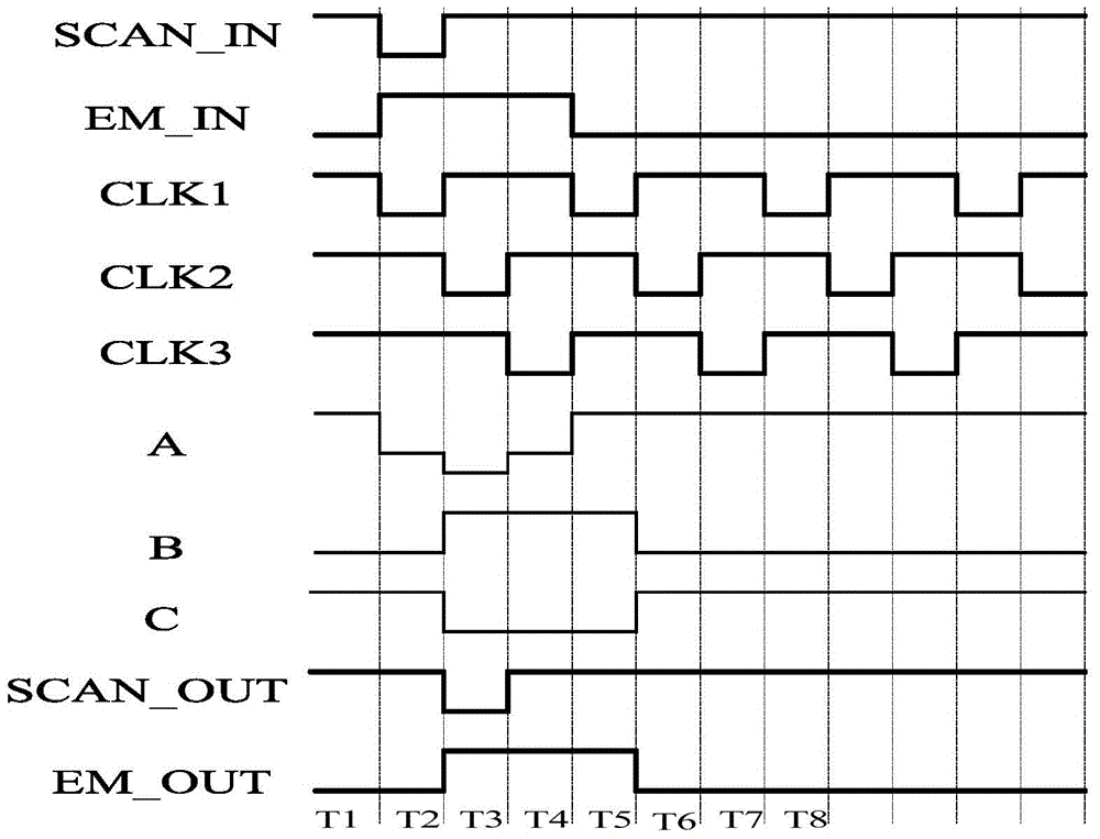
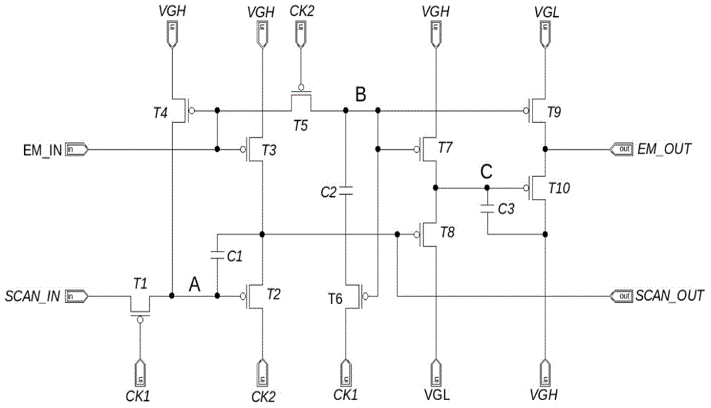
[0037] see figure 1 , figure 2 In one embodiment, a GOA unit circuit is provided, including: first to tenth thin film transistors, first to third capacitors, SCAN signal input terminals, EM signal input terminals, SCAN signal output terminals, and EM signal output terminals , first to third clock signal terminals, high-level terminals, low-level terminals, and circuit nodes A to C. Such as figure 1 , the specific circuit connection relationship is expressed as: the source of the first thin film transistor T1 is connected to the SCAN signal input terminal SCAN_IN, the gate is connected to the fi...


PUM


Abstract

The invention discloses a GOA unit circuit comprising first to tenth film transistors, first to third capacitors, a SCAN signal input end, an EM signal input end, a SCAN signal output end, an EM signal output end, first to third clock signal ends, a high level end, a low level end, and A to C circuit nodes. The invention also discloses a GOA circuit; the number of film transistors and capacitors needed by the GOA unit circuit can be reduced, and the output signal is stable with no offset.

Description

technical field [0001] The present invention relates to the field of display technology, in particular to a Gated Driver On Array (GatedriverOnArray, array substrate row driver) unit circuit and a GOA circuit. Background technique [0002] In the field of display technology, it is a well-known technology to drive pixel circuits to work by GOA circuits. Wherein, the GOA circuit is formed by cascading multiple GOA unit circuits, and each GOA unit circuit drives at least one row of pixels. [0003] The GOA unit circuit can provide two types of signals: [0004] (1) Scan (SCAN) signal. The scanning signal is mainly used to turn on the thin film transistors of the row of pixels for a certain period of time, so as to scan the row of pixels into the data signal and store it in the capacitance of the row of pixel circuits. The scan signal or its shift signal can also be used to initialize the potential of the capacitor, or initialize the anode of the OLED. [0005] (2) Emit (EMI...

Claims


Application Information

Patent Timeline
Patent Type & Authority Applications(China)
IPC IPC(8): G02F1/1345G09G3/32G09G3/36
CPCG02F1/13454G09G3/3225G09G3/3648
Inventor 胡中艺翁祖伟吴锦坤胡君文田栋协谢志生苏君海李建华
Owner TRULY HUIZHOU SMART DISPLAY
Why Eureka
Try Eureka