a display panel
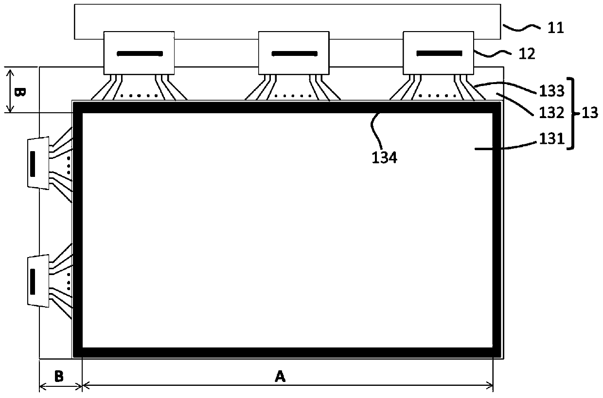
A technology of display panel and non-display area, applied in instruments, nonlinear optics, optics, etc., can solve the problems of increasing the frame width of the display device, not being light and beautiful in vision, affecting the integrity of the splicing screen, etc.
- Summary
- Abstract
- Description
- Claims
- Application Information
AI Technical Summary
Problems solved by technology
Method used
Image
Examples
Embodiment Construction
[0015] Below in conjunction with accompanying drawing and specific embodiment, further illustrate the present invention, should be understood that these embodiments are only for illustrating the present invention and are not intended to limit the scope of the present invention, after having read the present invention, those skilled in the art will understand various aspects of the present invention Modifications in equivalent forms all fall within the scope defined by the appended claims of this application.
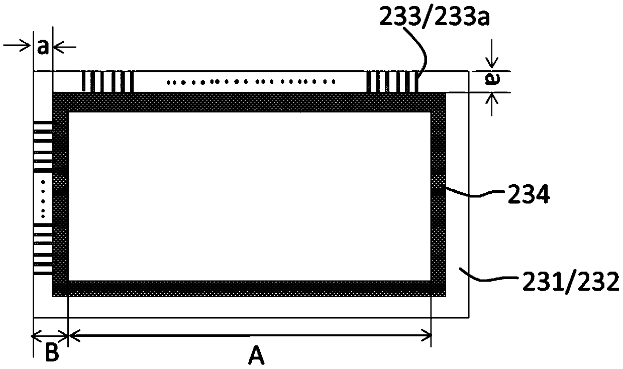
[0016] Such as Figure 2-Figure 4 The structure diagram of the display panel of the present invention is shown, the display panel includes a color filter substrate 231, a thin film transistor array substrate 232, a liquid crystal layer 235, a frame glue 234, a flexible circuit board 22 and a driver circuit board 21. The color filter substrate 231 is arranged opposite to the thin film transistor array substrate 232, the liquid crystal layer 235 is arranged between the co...
PUM
| Property | Measurement | Unit |
|---|---|---|
| thickness | aaaaa | aaaaa |
Abstract
Description
Claims
Application Information


