Supercharge Your Innovation With Domain-Expert AI Agents!

A display device and its manufacturing method

A technology for a display device and a manufacturing method, which is applied in semiconductor/solid-state device manufacturing, static indicators, instruments, etc., can solve problems such as voltage setting redundancy, voltage exceeding, and slash burrs, and achieve voltage and power consumption reduction, The effect of increasing the surface area and increasing the current density

Active Publication Date: 2018-09-25
WUHAN TIANMA MICRO ELECTRONICS CO LTD +1
View PDF7 Cites 0 Cited by
  • Summary
  • Abstract
  • Description
  • Claims
  • Application Information

AI Technical Summary

Problems solved by technology

[0010] 1. The calculation display effect is not as good as Real, such as the problem of slash glitches;
[0011] 2. The circuit (IC) will become complicated and increase a lot of cost;
[0012] 3. Lack of core algorithm patents
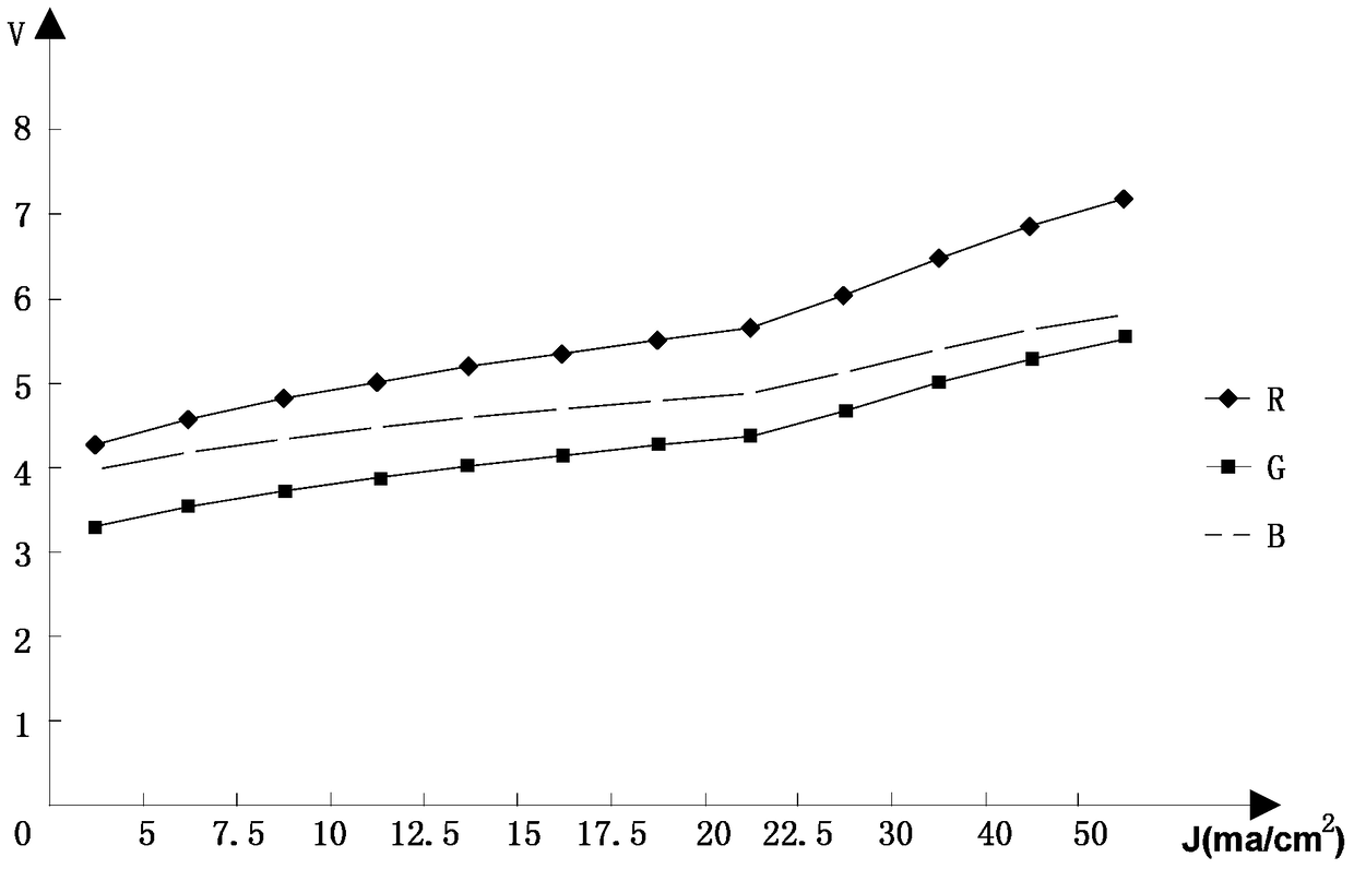
[0014] In addition, in the prior art, as far as an AMOLED panel is concerned, the overall cross-voltage design is generally certain, so this setting must leave enough buffer for the voltage of each sub-pixel, so that the voltage of each sub-pixel can be guaranteed
In this case, the voltage of some sub-pixels exceeds the required voltage, resulting in voltage setting redundancy, and the resulting waste of power consumption will become the bottleneck of the entire setting

Method used


Image

  • A display device and its manufacturing method
  • A display device and its manufacturing method
  • A display device and its manufacturing method

Examples


Embodiment Construction

[0063] Example embodiments will now be described more fully with reference to the accompanying drawings. Example embodiments may, however, be embodied in many forms and should not be construed as limited to the embodiments set forth herein; rather, these embodiments are provided so that this disclosure will be thorough and complete, and will fully convey the concept of example embodiments to those skilled in the art. The same reference numerals denote the same or similar structures in the drawings, and thus their repeated descriptions will be omitted.

[0064] The described features, structures, or characteristics may be combined in any suitable manner in one or more embodiments. In the following description, numerous specific details are provided in order to give a thorough understanding of embodiments of the invention. However, those skilled in the art will appreciate that the technical solutions of the present invention may be practiced without one or more of the specific...


PUM


Abstract

The invention provides a display device and a manufacturing method thereof. The display device includes: a backplane module, including a TFT-driven backplane and an insulating layer on the TFT-driven backplane; a pixel definition layer, a transparent conductive layer, and an organic light-emitting layer, forming On the insulating layer, the pixel definition layer includes a plurality of openings, the transparent conductive layer includes a transparent conductive layer in the opening area and a transparent conductive layer in the non-opening area, the transparent conductive layer in the opening area is located in the plurality of openings in the pixel definition layer, and the organic light-emitting layer forms On the transparent conductive layer in the opening area, a plurality of sub-pixels are correspondingly formed; in the backplane module below the sub-pixels of at least one color, there are three-dimensional concave holes, each three-dimensional concave hole corresponds to an opening, and the opening area The transparent conductive layer and the organic light-emitting layer are located in the three-dimensional concave hole. The invention changes the spatial structure of the pixel area, increases the surface area of ​​the light-emitting area, and is applicable to various display devices, so that the current density will not increase and the voltage and power consumption will be reduced under the condition of high PPI.

Description

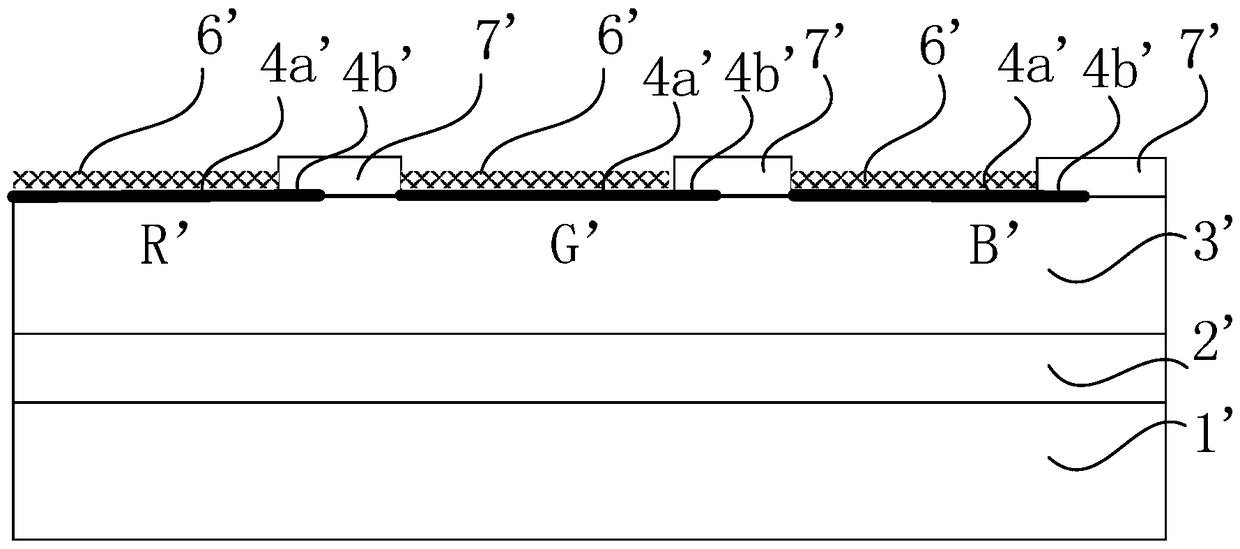
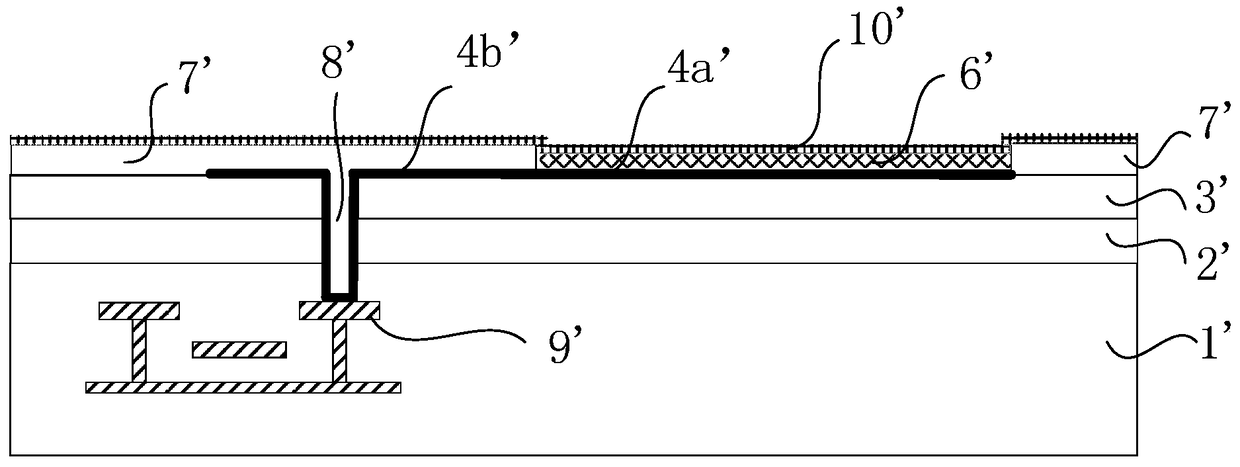
technical field [0001] The invention relates to a display device and a manufacturing method thereof, in particular to a low power consumption display device and a manufacturing method thereof. Background technique [0002] The pixel arrangement in the existing AMOLED panel is generally a real pixel arrangement (Real arrangement). The structure of this arrangement is relatively simple, the layout design and mask production are more convenient, and the process production is also easier. [0003] Such as Figure 1a As shown, a conventional AMOLED panel includes a backplane module 1', a passivation layer 2', a planarization layer 3', a pixel definition layer 7', a transparent conductive layer 4' and an organic light emitting layer 6'. Wherein the passivation layer 2' is formed on the backplane module 1', and the planarization layer 3' is formed on the passivation layer 2'. The pixel definition layer 7' is formed on the insulating layer, the pixel definition layer 7' includes a ...

Claims


Application Information

Patent Timeline
Patent Type & Authority Patents(China)
IPC IPC(8): H01L27/32H01L21/77
CPCH10K59/353H10K59/124H10K50/11H10K59/80521H10K59/80515H10K50/813H10K50/822H10K59/122H10K59/131H10K59/1201G09G3/3258G09G2300/0452G09G2300/0465G09G2300/0809G09G2330/021
Inventor 熊志勇
Owner WUHAN TIANMA MICRO ELECTRONICS CO LTD
Features
  • R&D
  • Intellectual Property
  • Life Sciences
  • Materials
  • Tech Scout
  • Unparalleled Data Quality
  • Higher Quality Content
  • 60% Fewer Hallucinations
Learn More