Semiconductor device
A semiconductor and conductive technology, which is applied in the direction of semiconductor devices, semiconductor/solid-state device parts, electric solid-state devices, etc., can solve problems such as drop, damage to the anode electrode and PIN diode adhesion, surge withstand drop, etc.
- Summary
- Abstract
- Description
- Claims
- Application Information
AI Technical Summary
Problems solved by technology
Method used
Image

Examples
no. 1 Embodiment approach
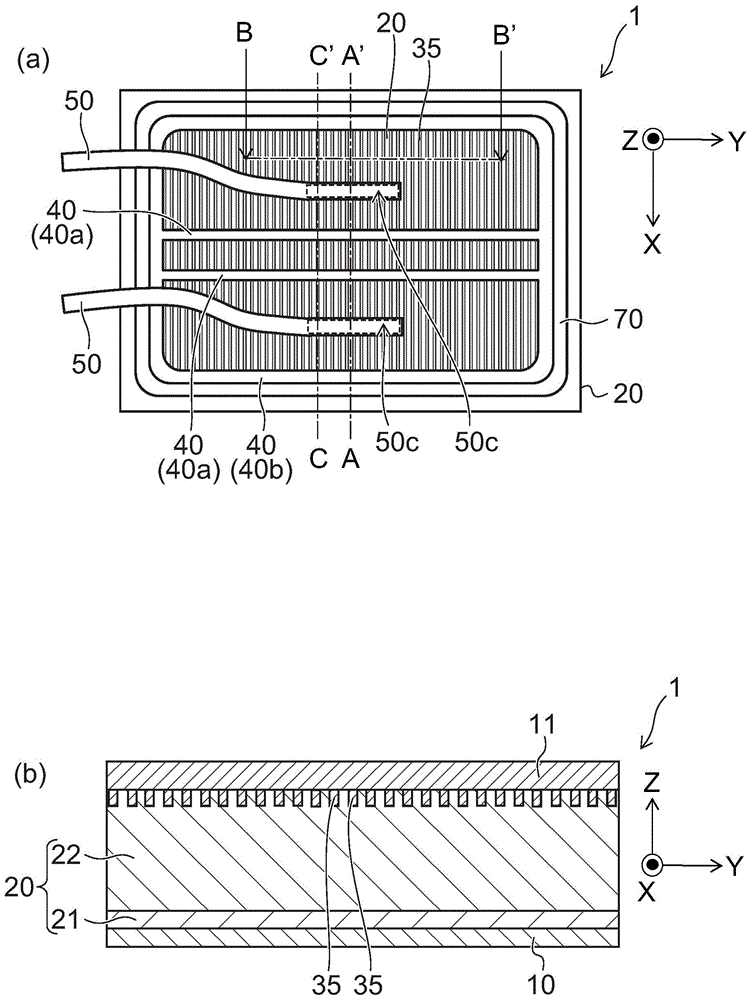
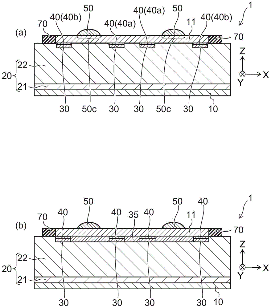
[0020] figure 1 (a) is a schematic plan view showing the semiconductor device according to the first embodiment, figure 1 (b) is a schematic cross-sectional view showing the semiconductor device according to the first embodiment.
[0021] figure 2 (a) and figure 2 (b) is a schematic cross-sectional view showing the semiconductor device according to the first embodiment.
[0022] here, in figure 1 (b) means figure 1 (a) BB' line section.
[0023] exist figure 2 In (a), it means that there is no configuration figure 1 The AA' line cross-section of the semiconductor region 35 in (a), at figure 2 In (b), it means that the configuration has figure 1 The BB' line cross section of the semiconductor region 35 in (a).
[0024] In addition, in figure 1 Not shown in (a) figure 1 (b) The anode electrode 11 shown.
[0025] Such as figure 1 (a)~ figure 2 As shown in (b), the semiconductor device 1 according to the first embodiment includes a cathode electrode 10 (first e...
no. 2 Embodiment approach
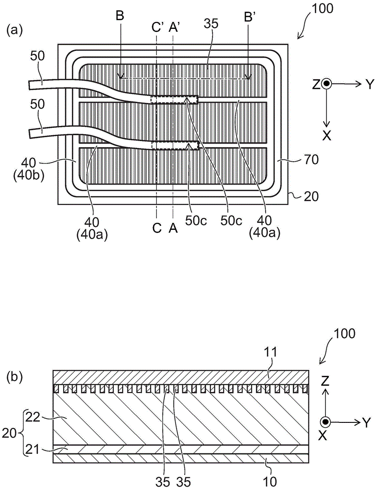
[0067] Figure 7 (a) is a schematic plan view showing a semiconductor device according to a first example of the second embodiment, Figure 7 (b) is a schematic plan view showing a semiconductor device according to a second example of the second embodiment.
[0068] Figure 8 (a) is a schematic plan view showing a semiconductor device according to a third example of the second embodiment, Figure 8 (b) is a schematic plan view showing a semiconductor device according to a fourth example of the second embodiment, Figure 8 (c) is a schematic plan view showing a semiconductor device according to a fifth example of the second embodiment.
[0069] exist Figure 7 In the semiconductor device 2 shown in (a), the adjacent bonding portions 50c are shifted in the Y direction and arranged in the X direction. Here, the distance d1 between the bonding portion 50c and the second region 40b and the distance d2 between the bonding portion 50c and the first region 40a may be substantially ...
no. 3 Embodiment approach
[0075] Figure 9 (a) is a schematic plan view showing a semiconductor device according to a first example of the third embodiment, Figure 9 (b) is a schematic plan view showing a semiconductor device according to a second example of the third embodiment.
[0076] exist Figure 9 In the semiconductor device 6 shown in (a), one wiring 50 has a plurality of bonding portions 50c. With such a structure, the number of wires 50 can be reduced. For example, the joint portions 50c aligned in the Y direction are connected by a loop-shaped connection portion 50rp. Also, the plurality of bonding portions 50 c are surrounded by the silicide regions 40 , respectively.
[0077] Here, the distance d1 between the joining portion 50c and the second region 40b and the distance d2 between the joining portion 50c and the portion 40aa of the first region 40a may be substantially the same. In addition, the distance d3 between the bonding portion 50c and the second region 40b and the distance d...
PUM
 Abstract
Description
Claims
Application Information
 - R&D Engineer
- R&D Manager
- IP Professional
- Industry Leading Data Capabilities
- Powerful AI technology
- Patent DNA Extraction
Browse by: Latest US Patents, China's latest patents, Technical Efficacy Thesaurus, Application Domain, Technology Topic.
© 2024 PatSnap. All rights reserved.Legal|Privacy policy|Modern Slavery Act Transparency Statement|Sitemap