A band-gap reference source circuit

A reference source circuit and power supply voltage technology, applied in the direction of adjusting electric variables, control/regulation systems, instruments, etc., can solve problems such as complex circuit structure, achieve simple circuit structure, eliminate triode zero current, and eliminate zero current.

Active Publication Date: 2016-02-10
SHANGHAI HUAHONG GRACE SEMICON MFG CORP
View PDF6 Cites 9 Cited by
  • Summary
  • Abstract
  • Description
  • Claims
  • Application Information

AI Technical Summary

Problems solved by technology

[0018] In the prior art, in order to enable the circuit to work directly at the third degeneracy point after power-on, an additional start-up circuit is required, and the circuit structure is complex

Method used


Image

  • A band-gap reference source circuit
  • A band-gap reference source circuit

Examples


Embodiment Construction

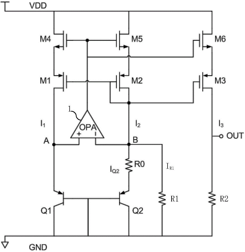
[0034] Such as figure 2 Shown is the circuit diagram of the bandgap reference source of the embodiment of the present invention. The bandgap reference source circuit of the embodiment of the present invention includes: three mirror current branches, three resistors R0, R1 and R2, two PNP transistors Q1 and Q2 and one op amp 1;

[0035] The current magnitudes of the three mirror current branches are proportional, and the currents provided by the three mirror current branches in the embodiments of the present invention are respectively I 1 , I 2 and I 3 .

[0036] The emitter area of ​​the second PNP transistor Q2 is N times the emitter area of ​​the first PNP transistor Q1, and N is greater than 1; this also makes the base-emitter voltage V of the first PNP transistor Q1 be1 greater than the base-emitter voltage of the first PNP transistor Q1 V be2 .

[0037] The emitter of the first PNP transistor Q1 is connected to node A, which is the output node of the first mirror c...


PUM


Abstract

The invention provides a band-gap reference source circuit comprising three mirror image current branches, three resistors, two PNP transistors and an operational amplifier. The emitting electrode area of the second PNP transistor is N times that of the first PNP transistor. The first PNP transistor is not connected with the resistors in parallel. Standard transistors are connected in series between the three mirror image current branches and a power supply voltage. The threshold electricity of the standard transistors is approximate to zero volt, so that the three mirror image current branches can be turned up when the power supply voltage is power on and degeneracy points of zero current of the whole circuit can be eliminated; the single-side bypass resistors are adopted and the first PNP transistor is not connected with the resistors in parallel, so that the first PNP transistor is directly turned on when the corresponding mirror image current branch is turned on and degeneracy points of zero current of audions can be eliminated. The circuit only has one stable working point, does not require additional start circuits, and is in simple in structure.

Description

technical field [0001] The invention relates to the manufacture of a semiconductor integrated circuit, in particular to a bandgap reference source circuit. Background technique [0002] Such as figure 1 Shown is the circuit diagram of the existing bandgap reference source; the existing bandgap reference source circuit includes: [0003] Three mirror current branches are composed of PMOS transistors M101, M102 and M103 respectively, and are used to provide proportional current I 101 , I 102 and I 103 . [0004] PNP transistor Q1 and PNP transistor Q102, the emitter area of ​​PNP transistor Q102 is larger than the emitter area of ​​PNP transistor Q101, so the base emitter voltage of PNP transistor Q101 is V be101 It must be greater than the base emitter voltage of the PNP transistor Q102, that is, V be102 The resistor R101 is connected between the emitter of the PNP transistor Q101 and the ground, one end of the resistor R102 is grounded, the other end is connected to th...

Claims


Application Information

Patent Timeline
Patent Type & Authority Applications(China)
IPC IPC(8): G05F3/26
Inventor 邵博闻唐成伟
Owner SHANGHAI HUAHONG GRACE SEMICON MFG CORP
Why Eureka
Try Eureka