Semiconductor structure

A technology of semiconductors and conductive wires, applied in the field of semiconductor structures, can solve problems such as power leakage and achieve the effect of reducing power leakage

Inactive Publication Date: 2016-02-10
MEDIATEK INC
View PDF2 Cites 0 Cited by
  • Summary
  • Abstract
  • Description
  • Claims
  • Application Information

AI Technical Summary

Problems solved by technology

This power leakage problem has become more severe with advances in semiconductor process technology leading to smaller IC dimensions

Method used


Image

  • Semiconductor structure
  • Semiconductor structure

Examples


Embodiment Construction

[0010] Certain terms are used throughout the description and claims to refer to particular components. Manufacturers may refer to components by different names, as those skilled in the art appreciate. This document does not intend to distinguish between parts that differ in name but have the same function. In the claims and the following description, the terms "comprises" and "comprises" are used in an open manner, and thus should be interpreted to mean "including, but not limited to". Also, the term "coupled" is intended to mean an indirect or direct electrical connection. Thus, if a device couples to another device, that connection may be through a direct electrical connection or through an indirect electrical connection via other devices and connections.

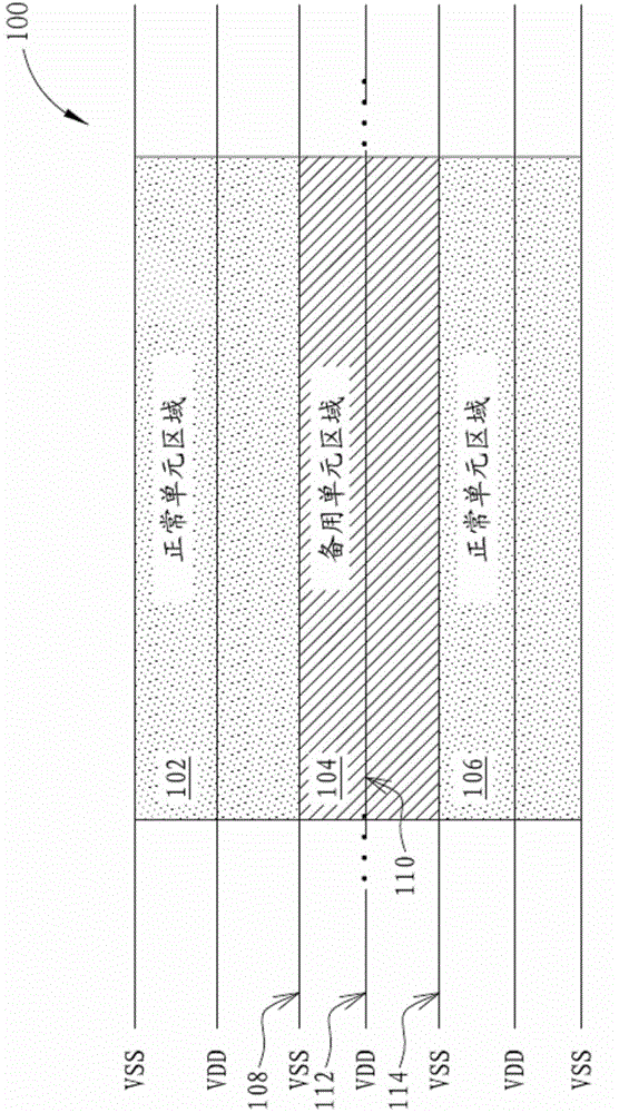
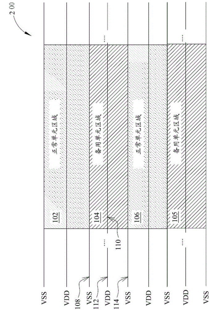
[0011] figure 1 is a layout diagram illustrating a semiconductor structure 100 according to an exemplary embodiment of the present invention. The semiconductor structure 100 includes a plurality of normal cell regions...


PUM


Abstract

A semiconductor structure includes a first spare cell region, a first conductive line and a second conductive line. The first spare cell region has a plurality of spare cells. The first conductive line is coupled between a first reference voltage and the plurality of spare cells, and is arranged for providing the first reference voltage to the plurality of spare cells of the first spare cell region. The second conductive line is coupled to a plurality of spare cells, and is arranged for providing a second reference voltage to the plurality of spare cells of the first spare cell region.

Description

【Technical field】 [0001] The present invention relates generally to semiconductor structures, and more particularly, to semiconductor structures having spare cell regions for reducing leakage power. 【Background technique】 [0002] A standard integrated circuit (Integrated Circuit, IC) includes a large number of electronic components, units, and circuit modules for implementing certain functions required by design specifications. These components, units, and circuit modules are generally constructed on a semiconductor substrate with overlapping metal layers, where conductive patterns ( ) are deployed as an interconnection network. Like properly functioning electronic components, ICs also have redundant or dummy cells that do not play an active role in the operation of the IC. Although spare cells may be designed to perform certain functions, according to the original circuit design of the IC, they are not connected to the normal operation of the electronic components, but ca...

Claims


Application Information

Patent Timeline
Patent Type & Authority Applications(China)
IPC IPC(8): H01L27/02
CPCH03K19/0016H01L27/0207H01L27/11807H03K19/1735
Inventor 傅志新张裕东
Owner MEDIATEK INC
Why Eureka
Try Eureka