Supercharge Your Innovation With Domain-Expert AI Agents!

Control circuit of SRAM array and SRAM

A storage array and control circuit technology, applied in the field of memory, can solve the problems of high difficulty and high cost of SRAM storage array, and achieve the effects of reducing energy consumption, improving programming ability, and reducing chip area

Active Publication Date: 2016-02-17
SPREADTRUM COMM (SHANGHAI) CO LTD
View PDF3 Cites 2 Cited by
  • Summary
  • Abstract
  • Description
  • Claims
  • Application Information

AI Technical Summary

Problems solved by technology

[0008] The problem solved by the present invention is that the cost and difficulty of performing the write operation of the existing SRAM storage array are high

Method used


Image

  • Control circuit of SRAM array and SRAM
  • Control circuit of SRAM array and SRAM
  • Control circuit of SRAM array and SRAM

Examples


Embodiment Construction

[0042] In order to make the above objects, features and advantages of the present invention more comprehensible, specific embodiments of the present invention will be described in detail below in conjunction with the accompanying drawings.

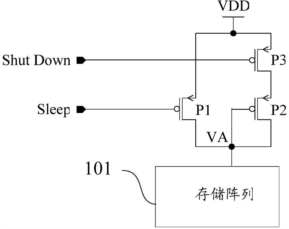
[0043] Such as Figure 4 As shown, the embodiment of the present invention provides a control circuit of the SRAM memory array 1, including: a first PMOS transistor P11, a conduction control unit 2 and at least one pull-down MOS transistor. In this embodiment, the number of pull-down MOS transistors is m as an example for illustration. The m pull-down MOS transistors include the first pull-down MOS transistor N1 . . . the m-th pull-down MOS transistor Nm.

[0044] The source of the first PMOS transistor P11 is suitable for inputting the first voltage VDD.

[0045] The drains of all the pull-down MOS transistors are connected to the drain of the first PMOS transistor P11, and the sources of all the pull-down MOS transistors are suitable fo...


PUM


Abstract

The invention discloses a control circuit of an SRAM array and an SRAM. The control circuit comprises a first PMOS transistor, a conduction control unit and at least one pull-down MOS transistor, wherein the source of the first PMOS transistor is suitable for inputting a first voltage; the drains of the pull-down MOS transistors are all connected with the drain of the first PMOS transistor, the sources of the pull-down MOS transistors are all suitable for inputting second voltages, and the voltage value of each second voltage is lower than the voltage value of the first voltage; and the conduction control unit is suitable for controlling all or part of the pull-down MOS transistors to be in conduction states within a predetermined time before the SRAM array enters a working state and performs a write operation.

Description

technical field [0001] The invention relates to the field of memory, in particular to a control circuit of an SRAM memory array and an SRAM memory. Background technique [0002] Static Random Access Memory (SRAM) has the advantageous feature of retaining data without needing to be updated. figure 1 It is a circuit diagram of an existing storage array power consumption control. The second PMOS is connected to the gate and drain of P2, which is equivalent to the function of a diode. When both the Sleep signal and the ShutDown signal are logic 0, both the first PMOS transistor P1 and the third PMOS transistor P3 are in the conduction state, and the conduction of the first PMOS transistor P1 can make the voltage at point VA equal to or very close to the power supply voltage VDD , at this time the storage array 101 enters a working state, and can perform read and write operations. [0003] When the Sleep signal is logic 1 and the ShutDown signal is logic 0, the first PMOS tran...

Claims


Application Information

Patent Timeline
IPC IPC(8): G11C11/413
Inventor 黄瑞锋郑坚斌于跃吴守道彭增发王林
Owner SPREADTRUM COMM (SHANGHAI) CO LTD
Features
  • R&D
  • Intellectual Property
  • Life Sciences
  • Materials
  • Tech Scout
  • Unparalleled Data Quality
  • Higher Quality Content
  • 60% Fewer Hallucinations
Learn More