Supercharge Your Innovation With Domain-Expert AI Agents!

Reaction chamber and semiconductor processing equipment

A reaction chamber and plasma technology, applied in discharge tubes, electrical components, circuits, etc., can solve the problem of high output power consumption of the excitation power supply, avoid density loss and energy attenuation, increase etching rate, and reduce consumption.

Active Publication Date: 2016-02-17
BEIJING NAURA MICROELECTRONICS EQUIP CO LTD
View PDF6 Cites 3 Cited by
  • Summary
  • Abstract
  • Description
  • Claims
  • Application Information

AI Technical Summary

Problems solved by technology

[0004] However, in practical applications, the following problems often occur: it is necessary to increase the etching rate to meet the requirements by increasing the output power of the excitation power supply used to generate plasma, which will cause high consumption of the output power of the excitation power supply.

Method used


Image

  • Reaction chamber and semiconductor processing equipment
  • Reaction chamber and semiconductor processing equipment

Examples


Embodiment Construction

[0021] In order to enable those skilled in the art to better understand the technical solution of the present invention, the reaction chamber and semiconductor processing equipment provided by the embodiments of the present invention will be described in detail below with reference to the accompanying drawings.

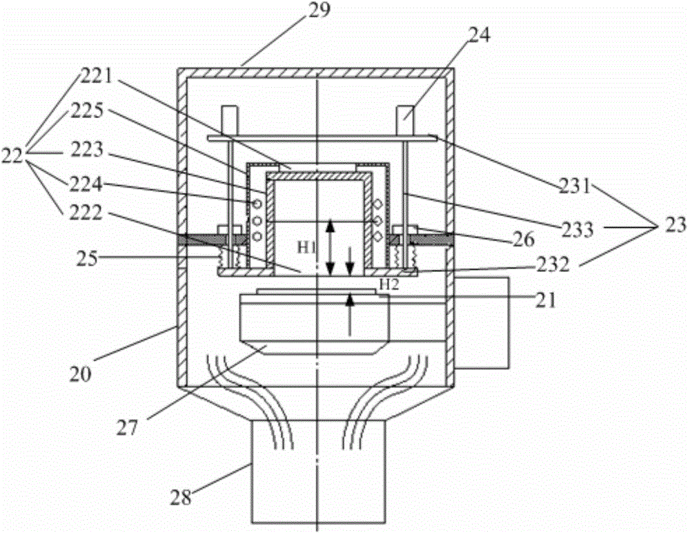
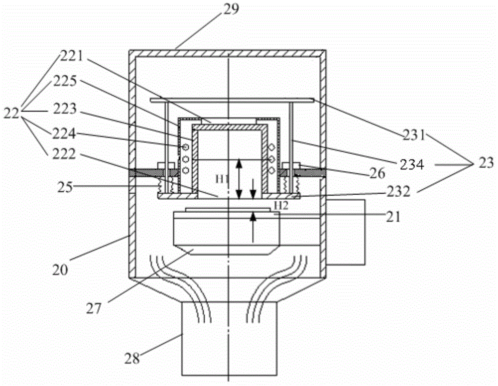
[0022] figure 1 Schematic diagram of the structure of the reaction chamber provided by the embodiment of the present invention. see figure 1 , the reaction chamber 20 provided in this embodiment includes a chuck 21 and a plasma generating device 22, the chuck 21 is arranged in the reaction chamber 20 for carrying the substrate S, and the chuck 21 includes an electrostatic chuck; the plasma generating device 22 Used to generate plasma and transport the plasma into the reaction chamber 20 . Specifically, such as figure 2 As shown, the plasma generating device 22 is provided with an input end 221 and an output end 222, the process gas enters the plasma generating dev...


PUM


Abstract

The invention provides a reaction chamber and semiconductor processing equipment. The reaction chamber comprises a chuck and a plasma generation device, wherein the chuck is arranged in the reaction chamber and is used for bearing a substrate, the plasma generation device is used for generating plasmas and conveying the plasmas into the reaction chamber, the reaction chamber further comprises a supporting member, and the supporting member is used for supporting the plasma generation device to make the plasma generation device penetrate through the top wall of the reaction chamber and make the plasma generation device be oppositely arranged relative to the chuck at a predetermined distance. According to the reaction chamber, density loss and energy attenuation are avoided in a plasma transmission process, so the etching rate can be improved, and consumption of an excitation power source can be reduced.

Description

technical field [0001] The invention belongs to the technical field of semiconductor equipment manufacturing, and in particular relates to a reaction chamber and semiconductor processing equipment. Background technique [0002] In the manufacturing process of integrated circuits, it is often necessary to use etching technology to make extremely fine-sized patterns on the substrate. In the reaction chamber of dry etching equipment, it generally includes a plasma system and a lower bias system. The plasma system is mainly used to generate high-density plasma in the reaction chamber; the lower bias system is mainly used to guide the plasma. The charged particles in the bulk bombard the substrate to complete the etching. [0003] With the development of three-dimensional stacked packaging, MEMS packaging, vertically integrated sensor arrays, and mesa MOS power device flip-chip bonding technology, through-silicon via (TSV) interconnection technology is receiving more and more at...

Claims


Application Information

Patent Timeline
Patent Type & Authority Applications(China)
IPC IPC(8): H01J37/20H01J37/32
Inventor 李璐
Owner BEIJING NAURA MICROELECTRONICS EQUIP CO LTD
Features
  • R&D
  • Intellectual Property
  • Life Sciences
  • Materials
  • Tech Scout
  • Unparalleled Data Quality
  • Higher Quality Content
  • 60% Fewer Hallucinations
Learn More