Nano step sample scanning measurement type scanning electron microscope

An electron microscope and nanotechnology, applied in scanning probe technology, instruments, etc., can solve the problems that cannot be predicted and controlled, and the measurement uncertainty evaluation of scanning electron microscope is difficult to carry out.

Active Publication Date: 2016-02-24
NAT INST OF METROLOGY CHINA
View PDF2 Cites 6 Cited by
  • Summary
  • Abstract
  • Description
  • Claims
  • Application Information

AI Technical Summary

Problems solved by technology

[0004] Since the conventional scanning electron microscope uses a coil to control the deflection of the electron beam to scan and obtain an image, the magnification and image distortion of the scanning electron microscope image are affected by the current image of the coil, and often cannot be predicted and controlled, making the measurement of the scanning electron microscope uncertain degree assessment is difficult

Method used


Image

  • Nano step sample scanning measurement type scanning electron microscope
  • Nano step sample scanning measurement type scanning electron microscope

Examples


Embodiment Construction

[0023] The present invention will be described in further detail below in conjunction with preferred embodiments.

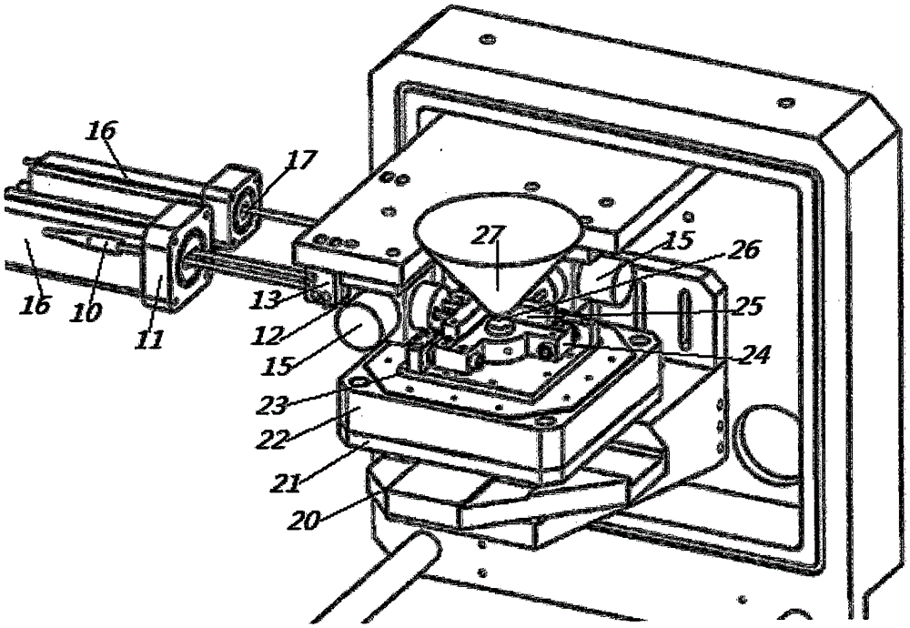
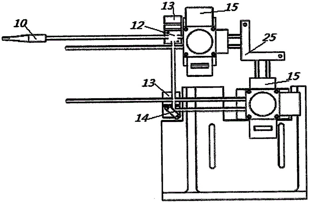
[0024] The present invention provides a nano-stepping sample scanning metrology scanning electron microscope including a high-speed nano-displacement scanning stage, a two-dimensional laser interferometer and an ultrasonic motor coarse-adjustment displacement stage, and the ultrasonic motor coarse-adjustment displacement stage does not include control electron beam deflection the coil. In order to reduce the impact of electron beam drift on the measurement, the ultrasonic motor coarse-adjustment displacement platform adopts a nano-displacement scanning platform with an elastic hinge system whose natural resonance frequency can reach more than 200 Hz when the load is 0.5 kg. The invention uses a two-dimensional laser interferometer to measure the position of the sample stage. The laser beams in two directions intersect with the electron beam of the electron micros...


PUM


Abstract

The invention relates to a nano step sample scanning measurement type scanning electron microscope. A two-dimensional laser interferometer comprises two interferometers, the interferometers are respectively positioned in the X direction and the Y direction of a measured sample, a light source for the interferometers is introduced from a laser through an optical fiber, penetrates through a vacuum window plate of a glass window and is split into two beams in the electron microscope, and the two beams of light are respectively incident to the two interferometers; when an ultrasonic motor rough adjustment displacement table performs scanning motion, a beam of emergent interference light is incident to a photoelectric detector through a vacuum window as an X-axis displacement data signal of the mobile station; the other beam of interference light is reflected by a flat reflector and then is incident to the interferometer close to a cabin door, and the emergent interference light is received by the other detector as a Y-axis displacement data signal of the mobile station; the X-axis and Y-axis displacement data are matched with the electron microscope to acquire secondary electronic signals exited by electron beams on the surface of the sample, thus obtaining measured data traced by the laser interferometer. The electron microscope can directly trace the measurement value to national standard meter.

Description

technical field [0001] The invention relates to the technical field of scanning electron microscopes, in particular to a nano-stepping sample scanning metrology scanning electron microscope. Background technique [0002] As an effective microstructure analysis tool, scanning electron microscope (SEM) can observe and analyze various forms of surfaces of various materials. The characteristics of the scanning electron microscope are: it can directly observe the surface structure of the sample; the depth of field is large, the image is full of three-dimensional effect; the image has a wide range of magnification and the resolution is relatively high; The other signals are used for micro-component analysis to observe various morphology features of the sample. [0003] Scanning electron microscopy usually uses a focused electron beam to scan point by point on the sample surface, interacting with the sample to generate secondary electrons, backscattered electrons, etc. The number...

Claims


Application Information

Patent Timeline
Patent Type & Authority Applications(China)
IPC IPC(8): G01Q30/20G01Q30/02
CPCG01Q30/02G01Q30/20
Inventor 高思田李伟施玉书李琪
Owner NAT INST OF METROLOGY CHINA
Why Eureka
Try Eureka