Three-dimensional semiconductor device and manufacturing method thereof

A device manufacturing method and semiconductor technology, which are applied in the fields of semiconductor/solid-state device manufacturing, semiconductor devices, electric solid-state devices, etc., can solve the problem of increasing the erasing and writing voltage, difficult to improve the coupling coefficient between control gate and floating gate, and maintaining characteristics of storage devices. and durability degradation to achieve the effect of improving device reliability

Inactive Publication Date: 2016-03-09
INST OF MICROELECTRONICS CHINESE ACAD OF SCI
View PDF3 Cites 17 Cited by
  • Summary
  • Abstract
  • Description
  • Claims
  • Application Information

AI Technical Summary

Problems solved by technology

In 3D NAND, the existing structure makes it difficult to increase the coupling coefficient from the control gate to the floating gate, which increases the erasing voltage and degrades the retention characteristics and durability of the storage device.

Method used


Image

  • Three-dimensional semiconductor device and manufacturing method thereof
  • Three-dimensional semiconductor device and manufacturing method thereof
  • Three-dimensional semiconductor device and manufacturing method thereof

Examples


Embodiment Construction

[0021] The features and technical effects of the technical solution of the present invention will be described in detail below with reference to the accompanying drawings and in conjunction with schematic embodiments, which discloses that the coupling coefficient from the control gate to the floating gate is effectively improved while reducing the coupling between vertical string units Semiconductor memory device and manufacturing method thereof. It should be pointed out that similar reference numerals represent similar structures, and the terms "first", "second", "upper", "lower" and the like used in this application can be used to modify various device structures or manufacturing processes . These modifications do not imply spatial, sequential or hierarchical relationships of the modified device structures or fabrication processes unless specifically stated.

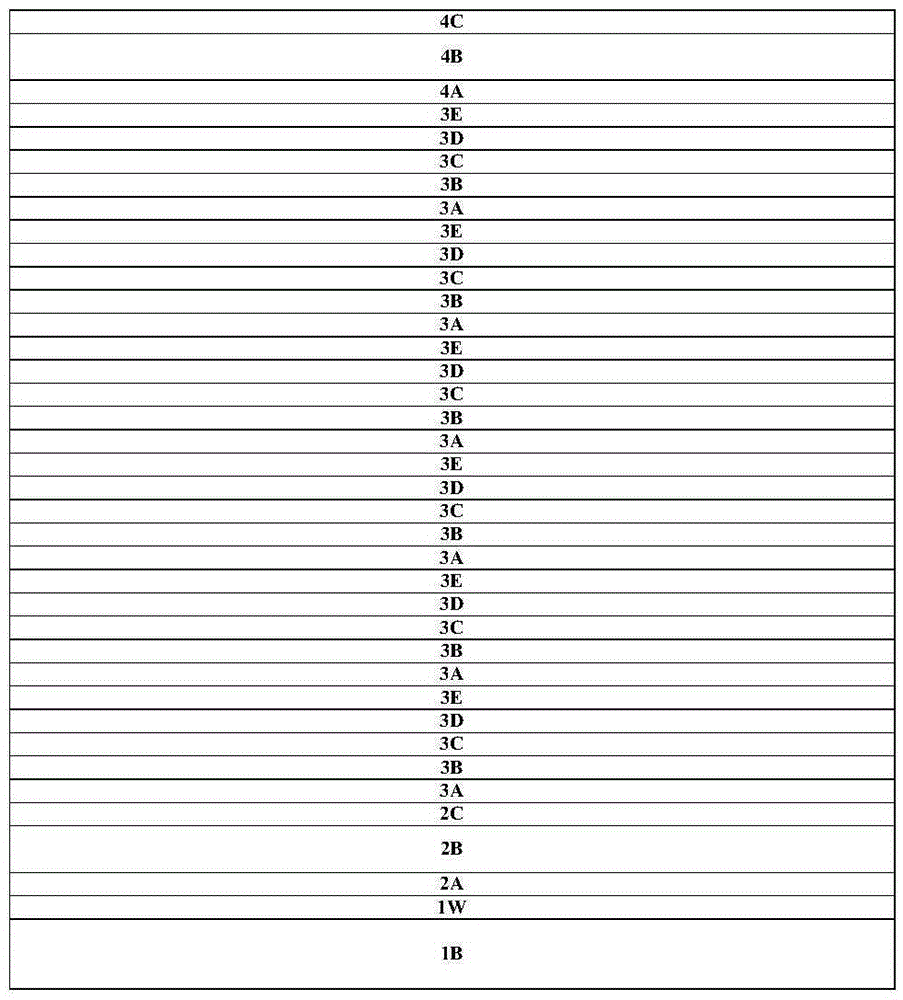
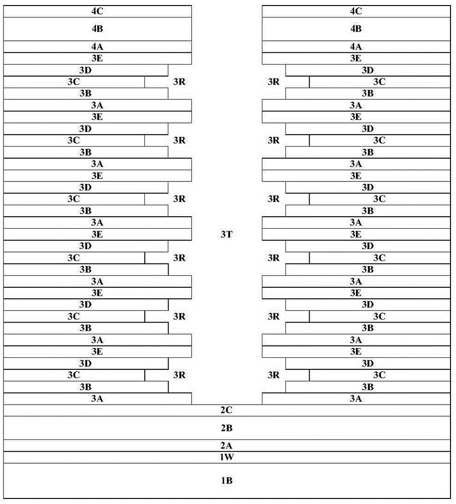
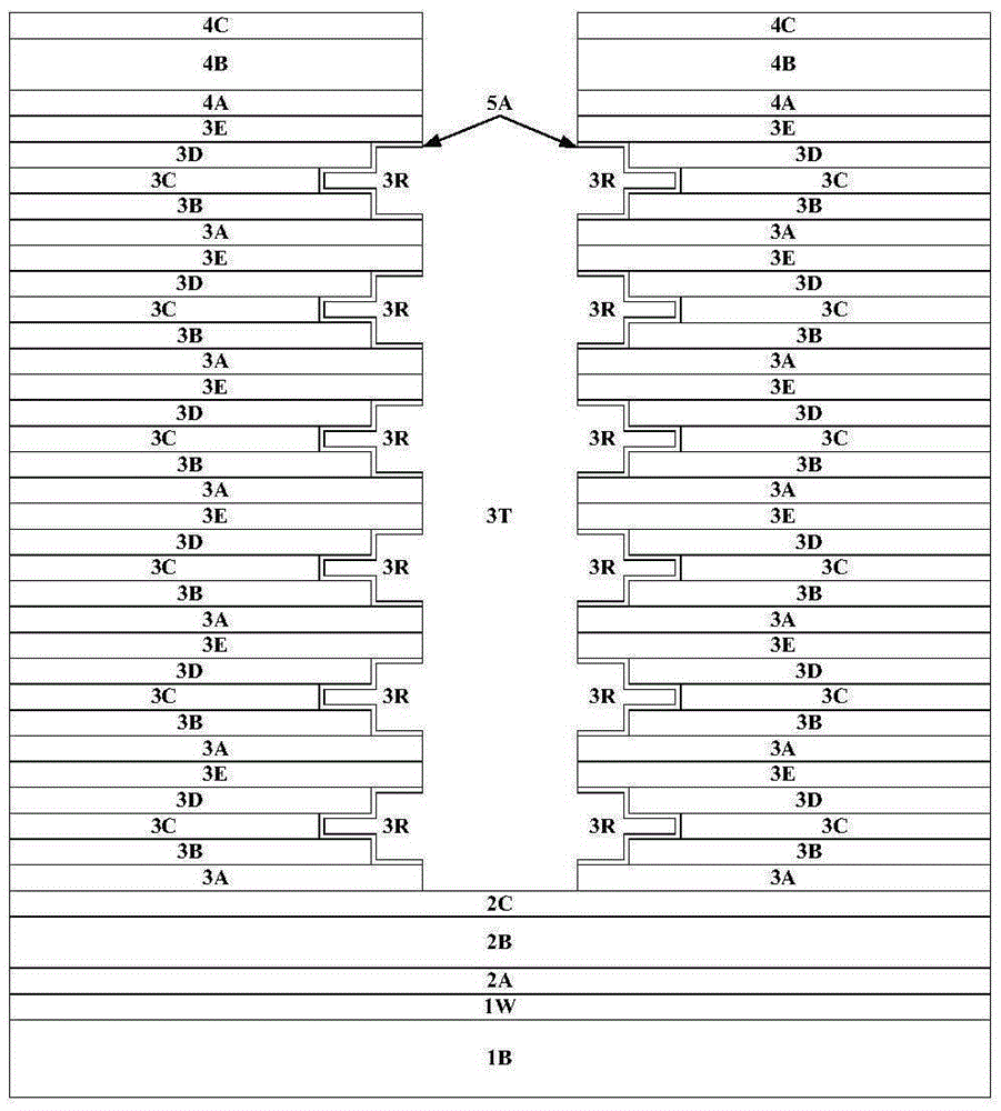
[0022] like figure 1 As shown, a plurality of stacks are formed on a substrate.

[0023] The substrate 1B is pro...


PUM


Abstract

The invention discloses a three-dimensional semiconductor device, which comprises multiple storage units. Each storage unit comprises a channel layer stack, multiple insulated layers, multiple pairs, a tunneling layer, a drain and a source, wherein the channel layer stack is distributed along the direction vertical to the surface of a substrate; the multiple insulated layers are alternately stacked along the side wall of the channel layer stack; the multiple pairs are formed by floating gates and control gates and horizontally and adjacently located between adjacent insulated layers, and at least one blocking layer exists between the floating gate and the control gate; the tunneling layer is located between the floating gate and the side wall of the channel layer stack; the drain is located at the top of the channel layer stack; the source is located on the substrate between adjacent two storage units of the multiple storage units; and the floating gates and the control gates are mutually matched to form a bent interface. According to the three-dimensional semiconductor device and the manufacturing method thereof, the control gates and the floating gates can be mutually engaged in the same horizontal level, the coupling coefficient from the control gates to the floating gates is effectively improved, coupling between vertical string units is reduced, and device reliability is improved.

Description

technical field [0001] The invention relates to a semiconductor device and a manufacturing method thereof, in particular to a three-dimensional semiconductor storage device and a manufacturing method thereof. Background technique [0002] In order to improve the density of memory devices, the industry has made extensive efforts to develop methods of reducing the size of two-dimensionally arranged memory cells. As the size of memory cells in two-dimensional (2D) memory devices continues to shrink, signal collisions and interference can increase significantly, making it difficult to perform multi-level cell (MLC) operations. In order to overcome the limitations of 2D memory devices, the industry has developed memory devices with a three-dimensional (3D) structure to increase integration density by three-dimensionally arranging memory cells on a substrate. [0003] Specifically, a multi-layer stacked structure (for example, multiple ONO structures alternating with oxides and n...

Claims


Application Information

Patent Timeline
Patent Type & Authority Applications(China)
IPC IPC(8): H01L27/115H01L21/8247H01L29/423
CPCH01L29/42336H01L29/4236H10B41/20H10B41/35H10B41/27
Inventor 霍宗亮叶甜春
Owner INST OF MICROELECTRONICS CHINESE ACAD OF SCI
Why Eureka
Try Eureka