Solar cell flip chip manufacturing method

A technology for solar cells and manufacturing methods, applied in final product manufacturing, sustainable manufacturing/processing, circuits, etc., can solve problems such as high cost and complex chip manufacturing process, and achieve the goal of reducing production costs, simplifying process technology, and improving production efficiency. Effect

Active Publication Date: 2016-03-09
兴数能源科技有限公司
View PDF6 Cites 6 Cited by
  • Summary
  • Abstract
  • Description
  • Claims
  • Application Information

AI Technical Summary

Problems solved by technology

However, compared with conventional triple-junction solar cells, the chip manufacturing process of flip-chip solar cells is more complicated, and the co

Method used


Image

  • Solar cell flip chip manufacturing method
  • Solar cell flip chip manufacturing method
  • Solar cell flip chip manufacturing method

Examples


Embodiment Construction

[0040] The following will clearly and completely describe the technical solutions in the embodiments of the present invention with reference to the accompanying drawings in the embodiments of the present invention. Obviously, the described embodiments are only some, not all, embodiments of the present invention. Based on the embodiments of the present invention, all other embodiments obtained by persons of ordinary skill in the art without making creative efforts belong to the protection scope of the present invention.

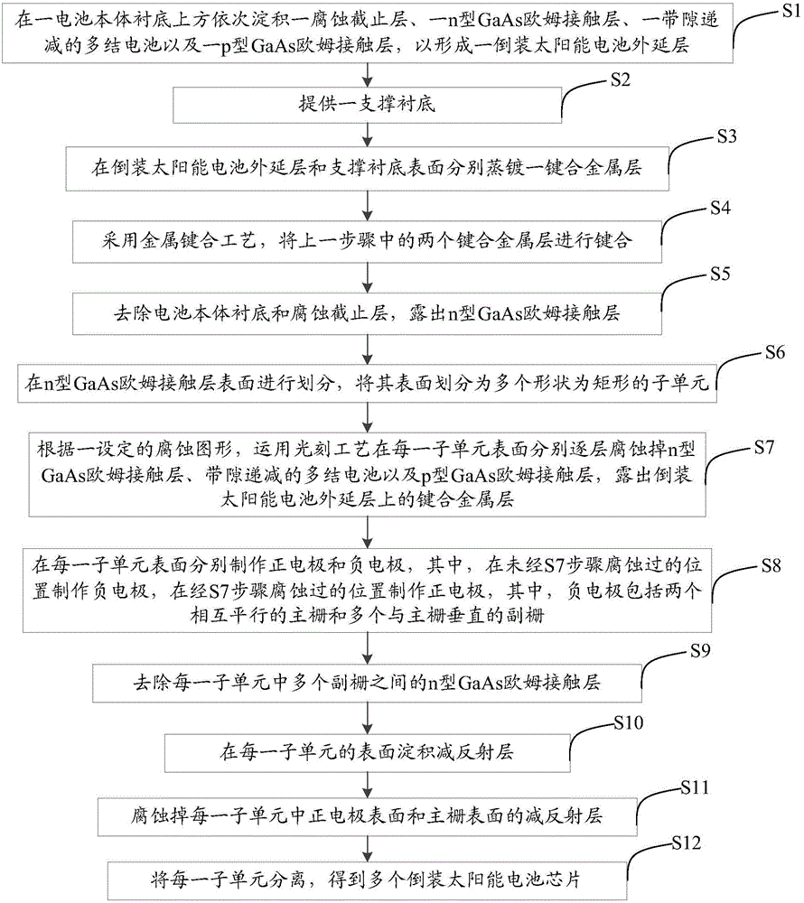
[0041] figure 1 It is a flowchart of a method for manufacturing a flip-chip solar cell chip according to an embodiment of the present invention; as shown in the figure, the method for manufacturing a flip-chip solar cell chip includes the following steps:

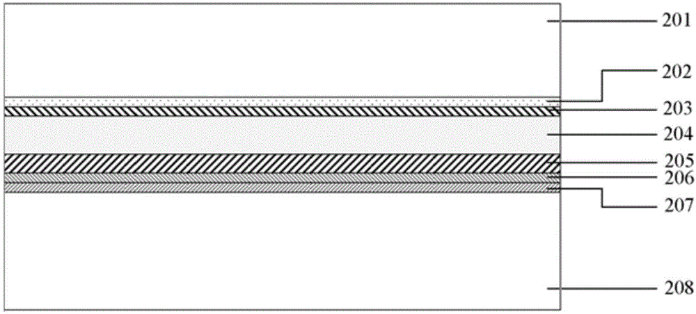
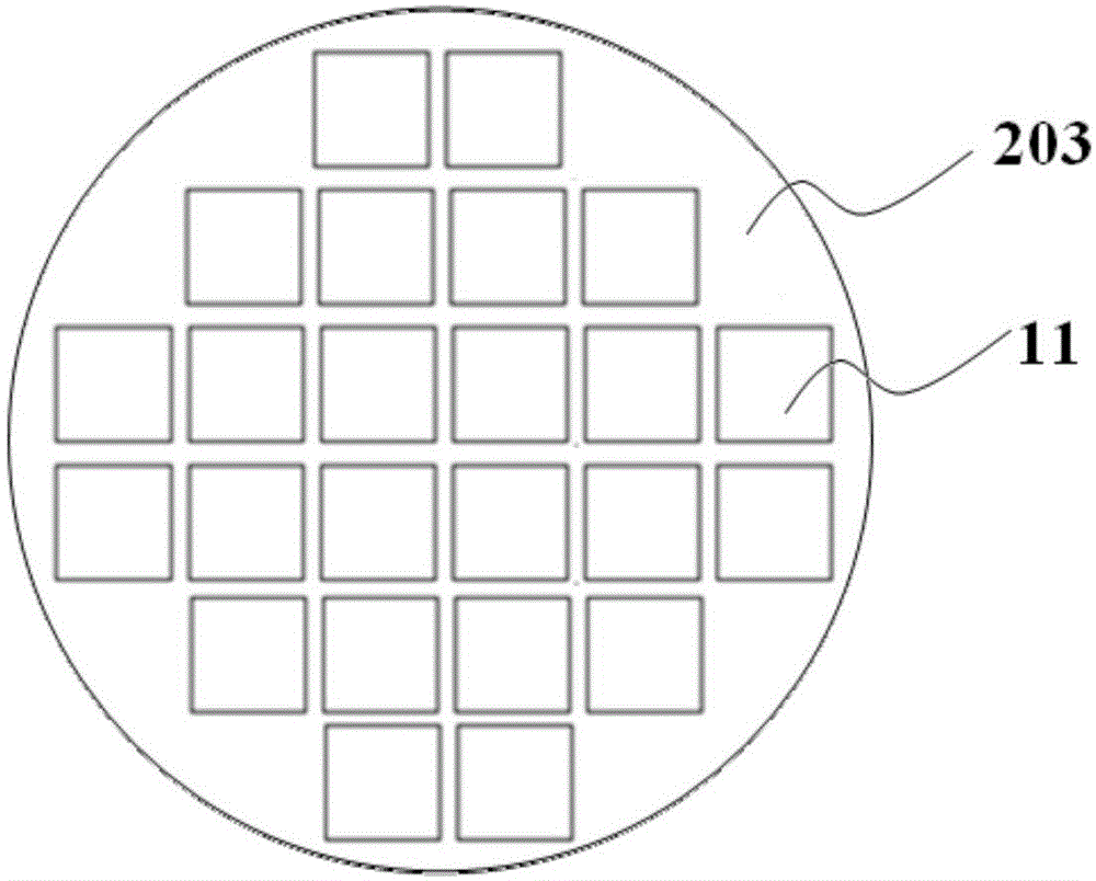
[0042] S1: Deposit an etch stop layer, an n-type GaAs ohmic contact layer, a multi-junction cell with decreasing gap, and a p-type GaAs ohmic contact layer sequentially over a cell body substrate to form a ...


PUM


Abstract

The invention relates to a solar cell flip chip manufacturing method, and the method comprises the following steps: forming an inverted solar cell epitaxial layer and a supporting substrate; respectively forming bonding metal layers on the inverted solar cell epitaxial layer and the surface of the supporting substrate in a vapor plating manner, and carrying out bonding; corroding an epitaxial layer substrate till an n-type GaAs ohmic contact layer is exposed; enabling the surface of the n-type GaAs ohmic contact layer to be divided into a plurality of sub-units; carrying out layer-by-layer corrosion on the surface of each sub-unit according to a set corrosion pattern till the bonding metal layer on the inverted solar cell epitaxial layer is exposed; respectively manufacturing a positive electrode and a negative electrode on the surface of each sub-unit, wherein the negative electrode comprises two parallel main grids and a plurality of auxiliary grids; removing the n-type GaAs ohmic contact layers among the plurality of auxiliary grids of each sub-unit; depositing an antireflection layer on the surface of each sub-uni; corroding the antireflection layers on the surfaces of the positive electrodes and the surfaces of the main grids of all sub-units; separating each sub-unit, and obtaining a plurality of solar cell flip chips.

Description

technical field [0001] The invention relates to the technical field of manufacturing semiconductor devices, in particular to a method for manufacturing flip-chip solar cell chips. Background technique [0002] Due to the non-renewability of fossil fuels and the environmental problems they cause, the development of renewable energy has become a global issue. Solar cells can directly convert solar energy into electrical energy, which greatly reduces people's dependence on fossil fuels, so the development of solar cells has far-reaching strategic significance. In recent years, with the development of concentrated photovoltaic technology, multi-junction III-V compound semiconductor solar cells have attracted more and more attention due to their high photoelectric conversion efficiency. [0003] Compared with the state-of-the-art GaInP / Ga(In)As / Ge conventional triple-junction cells with lattice matching, the flip-chip heterogeneously grown multi-junction cells have the advantage...

Claims


Application Information

Patent Timeline
IPC IPC(8): H01L31/18
CPCY02P70/50
Inventor 武智平
Owner 兴数能源科技有限公司
Why Eureka
Try Eureka