biased electrostatic discharge (ESD) circuit and method reducing capacitance of ESD circuit
An electrostatic discharge and circuit technology, applied in the field of electrostatic discharge protection, can solve problems such as damage to electronic devices
- Summary
- Abstract
- Description
- Claims
- Application Information
AI Technical Summary
Problems solved by technology
Method used
Image
Examples
Embodiment Construction
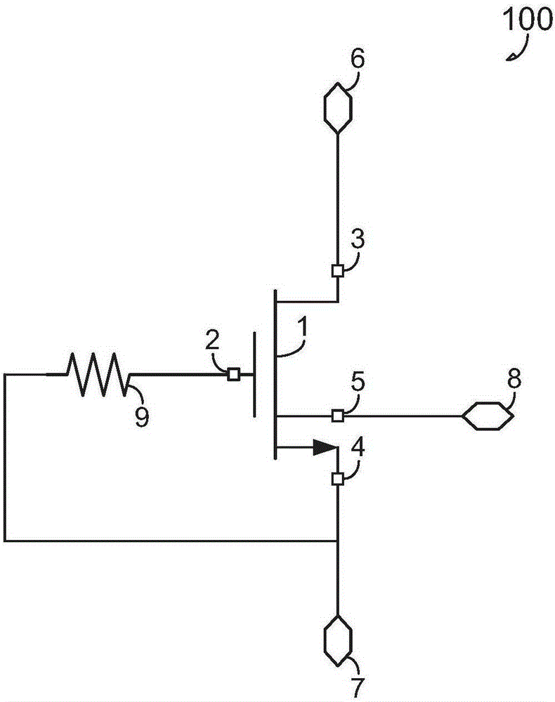
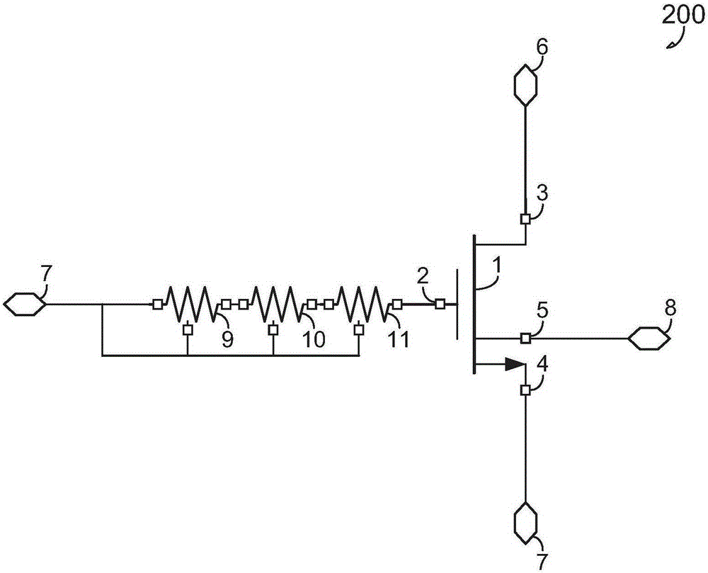
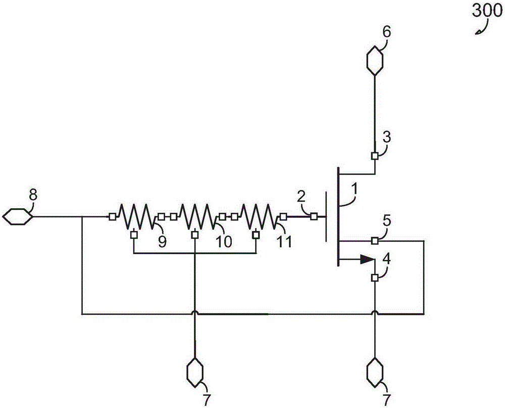
[0010] The present inventors have also recognized, among other things, that a bias voltage can be applied to an electrostatic discharge (ESD) structure, such as a well region or a gate in an ESD structure, to reduce the capacitance of the ESD structure, while other ESD structures Parameters vary little to no.
[0011] Figure 1-Figure 3 An exemplary biased electrostatic discharge (ESD) circuit configured to provide an ESD path to ground through an ESD device 1 such as an n-type metal oxide semiconductor (NMOS) transistor is generally shown, the circuit having a gate terminal 2 , drain terminal 3, source terminal 4, and body terminal 5 (eg, p-epi / p body terminal). Figure 1-Figure 3 The bias ESD circuit uses a negative voltage applied (e.g., externally) to the body terminals (e.g., p-epi / p body) of the ESD device to reduce the source / drain capacitance of the ESD device (e.g., n+ source / drain electrode-to-body capacitance), thereby reverse-biasing the well region to the drain ca...
PUM
 Abstract
Description
Claims
Application Information
 - R&D Engineer
- R&D Manager
- IP Professional
- Industry Leading Data Capabilities
- Powerful AI technology
- Patent DNA Extraction
Browse by: Latest US Patents, China's latest patents, Technical Efficacy Thesaurus, Application Domain, Technology Topic, Popular Technical Reports.
© 2024 PatSnap. All rights reserved.Legal|Privacy policy|Modern Slavery Act Transparency Statement|Sitemap|About US| Contact US: help@patsnap.com


