Method for improving electroplating uniformity of package substrate

A packaging substrate and uniformity technology, applied in the direction of circuits, electrical components, electric solid devices, etc., can solve the problems of poor plating uniformity, uneven distribution of plating patterns, etc., to improve quality assurance, improve plating uniformity, and improve production efficiency Effect

Inactive Publication Date: 2016-03-16
NAT CENT FOR ADVANCED PACKAGING
View PDF7 Cites 10 Cited by
  • Summary
  • Abstract
  • Description
  • Claims
  • Application Information

AI Technical Summary

Problems solved by technology

[0008] In view of the problems of poor plating uniformity caused by uneven distribution of plating patterns in the above and / or existing semiconductor packages, the present invention is proposed

Method used


Image

  • Method for improving electroplating uniformity of package substrate
  • Method for improving electroplating uniformity of package substrate
  • Method for improving electroplating uniformity of package substrate

Examples


Embodiment Construction

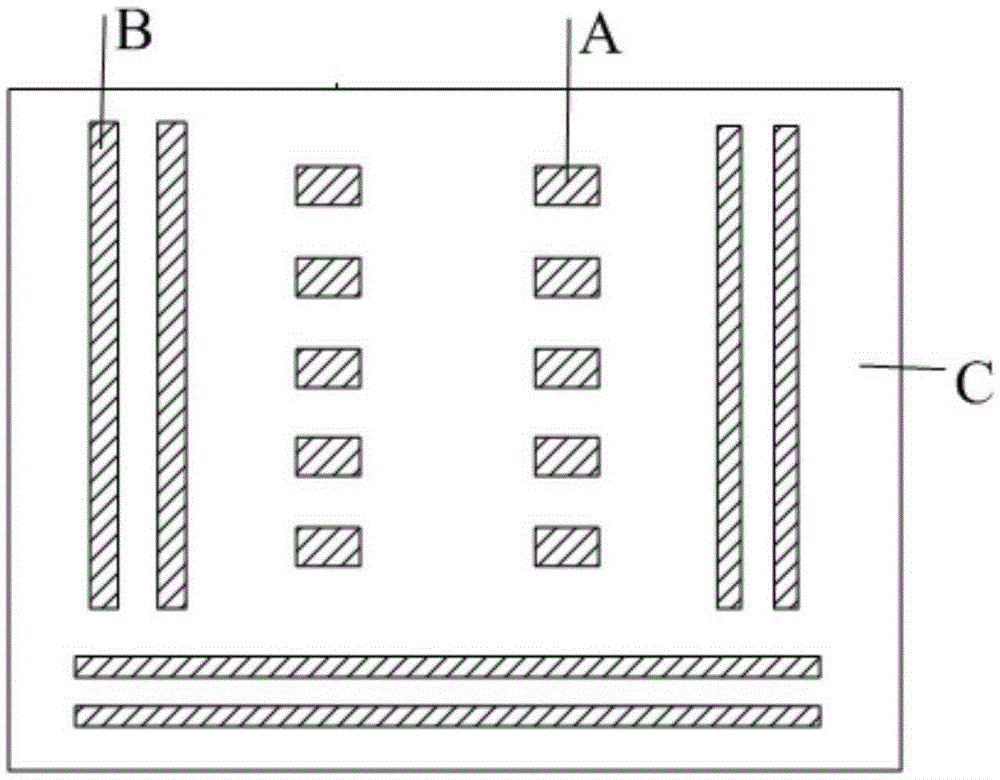
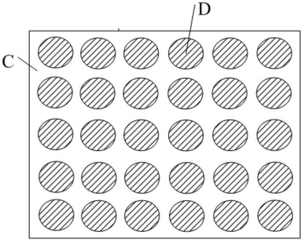
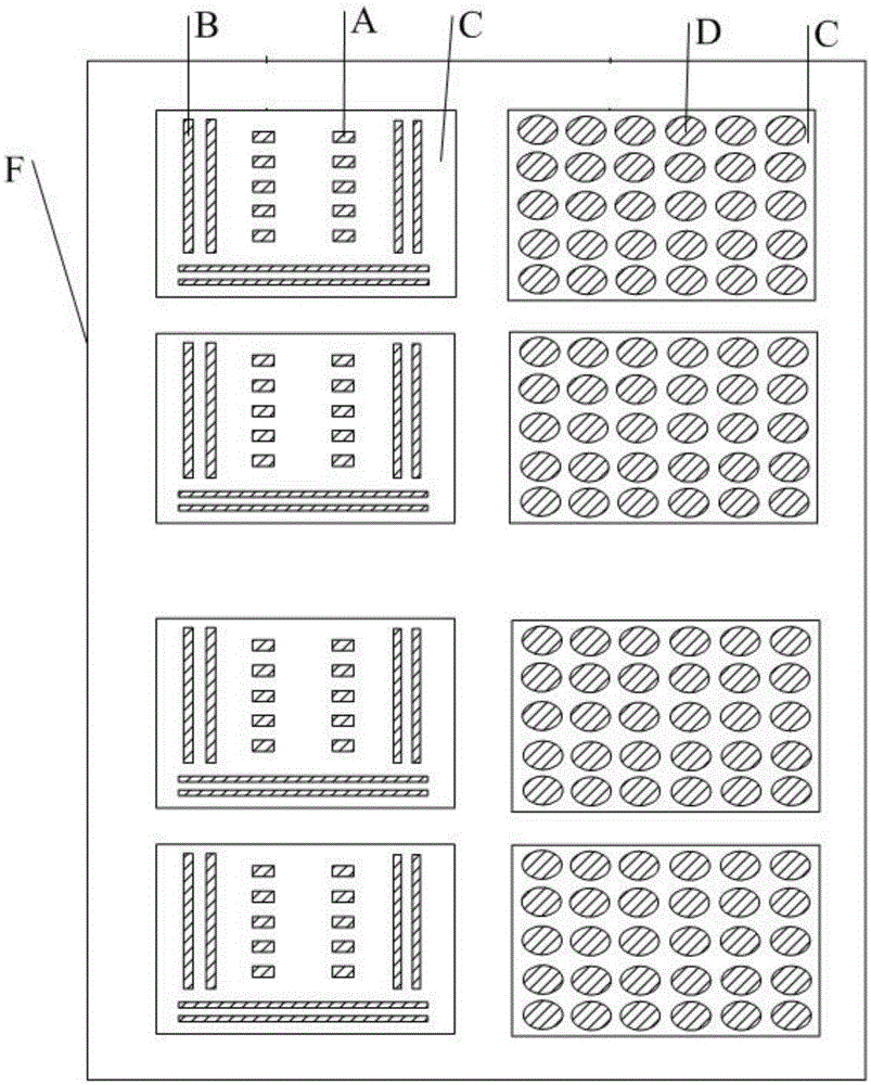
[0026] In order to make the above objectives, features and advantages of the present invention more obvious and understandable, the specific embodiments of the present invention will be further described below in conjunction with specific drawings.

[0027] In the following description, many specific details are explained in order to fully understand the present invention. However, the present invention can also be implemented in other ways different from those described here. Those skilled in the art can do so without departing from the connotation of the present invention. Similar promotion is made, so the present invention is not limited by the specific embodiments disclosed below.

[0028] Secondly, the present invention will be described in detail in conjunction with schematic diagrams. In detailing the embodiments of the present invention, for ease of description, the cross-sectional view showing the device structure will not be partially enlarged according to the general scal...


PUM

PropertyMeasurementUnit
sizeaaaaaaaaaa
distanceaaaaaaaaaa

Abstract

The invention relates to a method for improving the electroplating uniformity of a package substrate. The method comprises the following steps that (1), a top layer graph of a unit plate comprises a chip binding bonding pad and a fine circuit, and the base material area, except for the chip binding bonding pad and the fine circuit, of the unit plate is a copper-free area; (2), a bottom layer graph of the unit plate comprises a ball-mounting package bonding pad, and the base material area, except for the ball-mounting package bonding pad, of the unit plat is a copper-free area; (3), plate splicing is performed, particularly, the analysis result of the graph structures of the top layer and the bottom layer of the unit plate shows that the designed graph of the top layer of the unit plate is sparser than the graph of the bottom layer, namely the copper content of the graph of the top layer of the unit plate is smaller than that of the graph of the bottom layer, and during plate splicing, multiple unit plates are arranged on a production plate, and the adjacent unit plates on the left and right sides are arranged in a mirroring mode; and (4) an electroplating process is conducted. The phenomenon of poor electroplating uniformity is solved through the method of changing spliced plates, and the electroplating uniformity of the package substrate is improved.

Description

Technical field [0001] The invention relates to a method for improving the plating uniformity of a package substrate, and belongs to the technical field of semiconductors. Background technique [0002] With the continuous development of packaging substrates in the direction of lightness, thinness, short size, and high density, processing capabilities have brought higher requirements to many devices; in terms of design, for different packaging forms, substrate design solutions have also become diversified. Due to the current packaging substrate design, the electroplating patterns are not uniformly distributed. Some substrate designs have only isolated pads or fine lines, while the area of ​​other parts may be too large; more common packaging substrate designs are the top layer of the substrate. The chip is connected through the wirebonding process, while the bottom layer of the substrate and other circuit boards are packaged in BGA (solder ball process). The most common problem wi...

Claims


Application Information

Patent Timeline
Patent Type & Authority Applications(China)
IPC IPC(8): C25D7/12H01L23/492
CPCC25D7/12H01L23/492
Inventor 宋阳
Owner NAT CENT FOR ADVANCED PACKAGING
Why Eureka
Try Eureka