

Abnormality detection device for power switch
A technology of power switch and abnormal detection, which is applied in the direction of circuit breaker testing, etc., and can solve problems such as failure and abnormal temperature rise
- Summary
- Abstract
- Description
- Claims
- Application Information
AI Technical Summary
Problems solved by technology
Method used
Image

Examples
Embodiment Construction
[0019] Below in conjunction with accompanying drawing, structural principle and working principle of the present invention are specifically described:
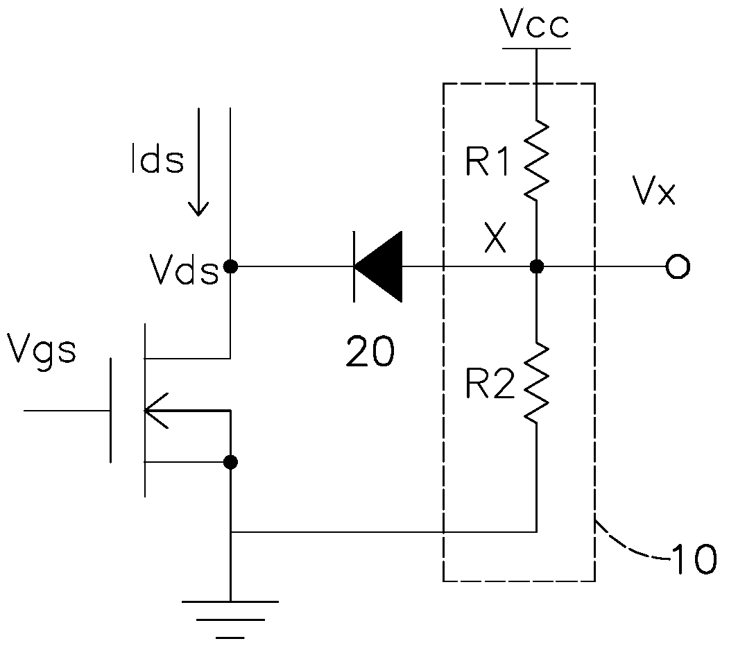
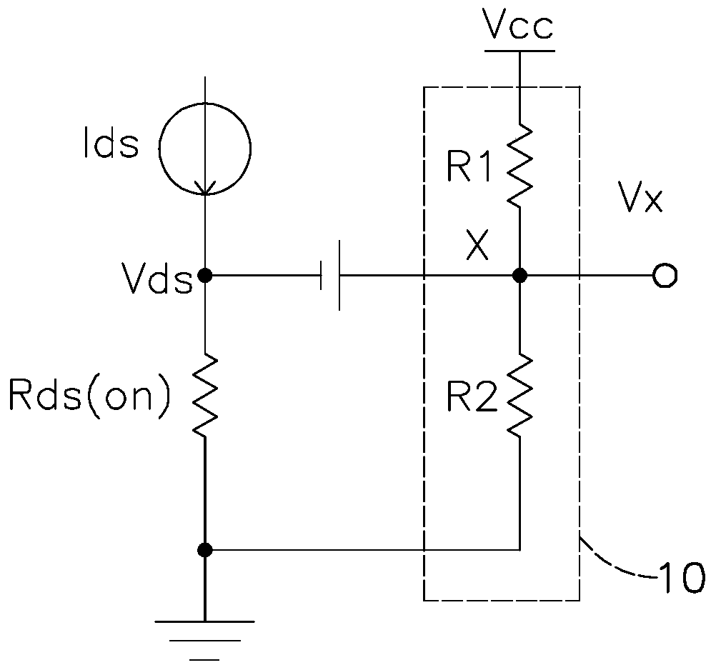
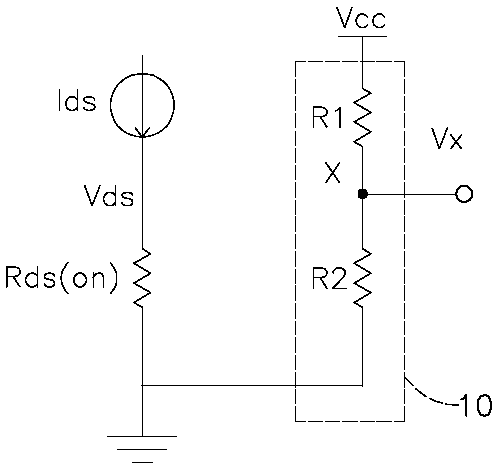
[0020] Regarding the abnormal detection device of the power switch of the present invention, a preferred embodiment thereof, please refer to figure 1 , the abnormal detection device of the power switch is connected on a current path of a power switch S1, and includes:
[0021] A voltage divider circuit 10, having a voltage divider node X;
[0022] A differential pressure switch 20 is connected between the voltage dividing node X of the voltage dividing circuit 10 and the current path of the power switch S1.
[0023] In this embodiment, the power switch S1 is a metal oxide semiconductor field effect transistor (MOSFET), more specifically, an N-type metal oxide semiconductor field effect transistor (NMOS). It must be noted that: the aforementioned NMOS field effect transistor is just an example, and is not intended to limit t...
PUM
 Abstract
Description
Claims
Application Information