Wet etching protection clamp free of damage to wafer

A technology for wet etching and protecting fixtures, applied in the manufacturing of electrical components, circuits, semiconductor/solid-state devices, etc., can solve the problems of small stress in the sealing part, wafer splintering, and troublesome use, so as to avoid damage to the wafer and avoid splintering. , low cost effect

Inactive Publication Date: 2016-03-16
ZHEJIANG UNIV
View PDF8 Cites 12 Cited by
  • Summary
  • Abstract
  • Description
  • Claims
  • Application Information

AI Technical Summary

Problems solved by technology

[0007] Some of the existing wet corrosion protection fixtures require cumbersome vacuuming devices, which are costly and relatively troublesome to use; some structur

Method used


Image

  • Wet etching protection clamp free of damage to wafer
  • Wet etching protection clamp free of damage to wafer
  • Wet etching protection clamp free of damage to wafer

Examples


Embodiment Construction

[0048] The specific embodiments of the present invention will be described below in conjunction with the accompanying drawings.

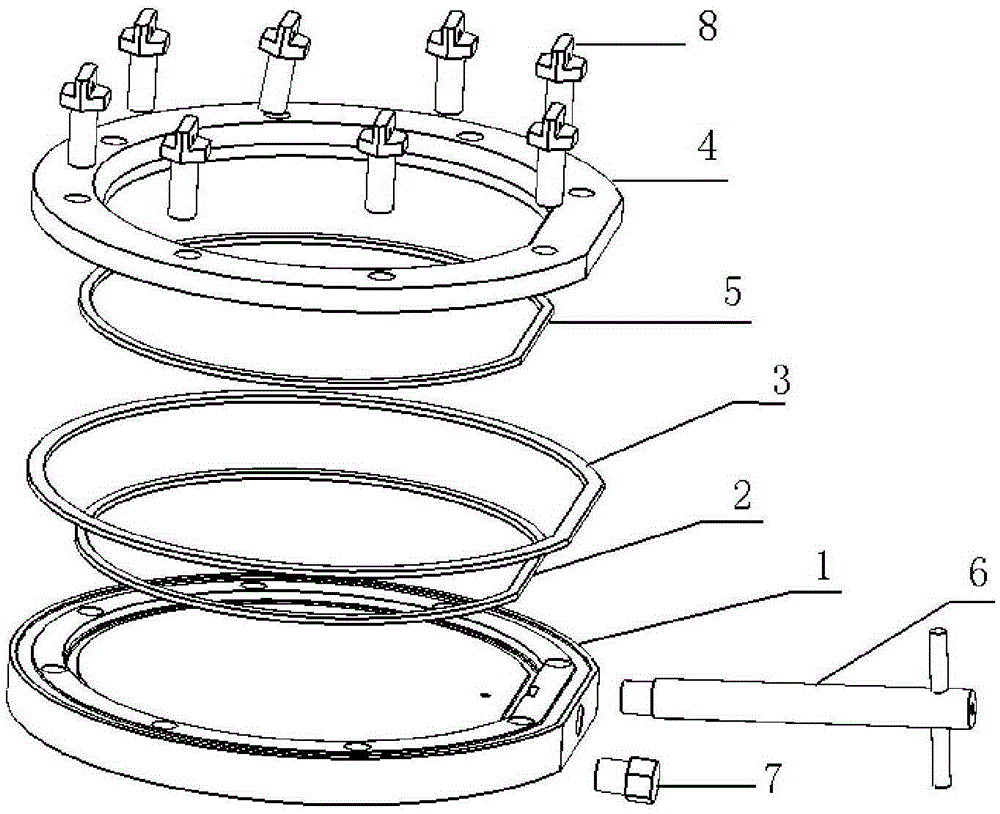
[0049] Such as figure 1As shown, a non-destructive wafer wet corrosion protection fixture includes a base 1 and a top cover 4 that cooperate with each other to clamp the wafer. The wafer includes a front side to be protected and a back side to be corroded, and the base accommodates And sealing and wrapping the front side, the top cover 4 is ring-shaped and presses against the edge of the back side, and both the base 1 and the top cover 4 are in contact with the wafer through an elastic buffer seal.

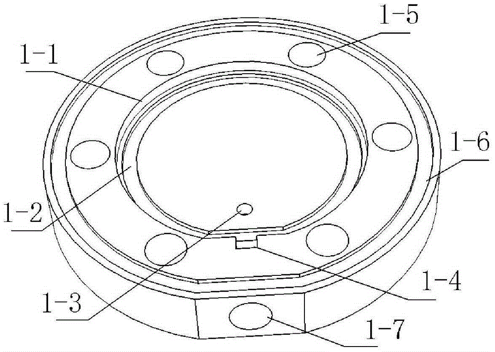
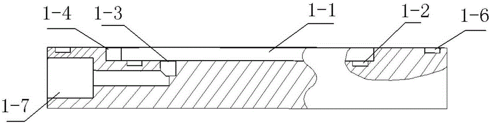
[0050] The non-destructive wafer corrosion protection jig has the advantages of low cost, convenient use, good sealing performance and no damage to the wafer. Its structure specifically includes a base 1 , a lower seal 2 , a balance washer 3 , a top cover 4 , an upper seal 5 , a ventilation handle 6 , a seal plug 7 and bolts 8 .

[0051] Such as Fig...


PUM


Abstract

The invention discloses a wet etching protection clamp free of a damage to a wafer. The wet etching protection clamp comprises a base and a head cover, wherein the base and the head cover are matched with each other to clamp the wafer; the wafer comprises a to-be-protected front surface and a to-be-corroded back surface; the base can accommodate and can wrap the front surface in a sealing manner; the head cover is in an annular shape and abuts on the edge part of the back surface; and the base and the head cover both are in contact with the wafer through elastic buffer sealing elements. The wet etching protection clamp has the advantages that due to a flexible clamping design, the wafer only contacts the flexible sealing element in use and the damage to the wafer caused by a rigid contact is reduced; due to a corresponding clamping design, clamping stress points of the upper and lower sealing elements correspond to each other, and the crack of the wafer caused by uneven stress is avoided; and due to the design of a corresponding shape of the protected surface, splitting caused by the uneven stress due to the fact that the wafer is twisted when the clamp is fastened is avoided.

Description

technical field [0001] The invention relates to the field of semiconductor manufacturing, in particular to a non-damaging wafer corrosion protection fixture. Background technique [0002] Wafer refers to the silicon wafer used in the production of silicon semiconductor integrated circuits. Because of its circular shape, it is called a wafer; it can be processed into various circuit element structures on the silicon wafer, and become an IC with specific electrical functions. product. [0003] In the process of semiconductor integrated circuit manufacturing and MEMS chip processing wafer, wet etching process is a very common process. However, when only one side of the wafer needs to be chemically wet etched, it is necessary to effectively protect the structure on the other side from being damaged by the etching solution. Usually, wet corrosion protection glue, high-temperature paraffin or black glue can be applied by spin coating, but wet corrosion protection glue is very ex...

Claims


Application Information

Patent Timeline
IPC IPC(8): H01L21/687
CPCH01L21/68714H01L21/68735H01L21/68785
Inventor 杨青徐鹏飞
Owner ZHEJIANG UNIV
Why Eureka
Try Eureka