A kind of preparation method and structure of Gan-based laser

A technology of lasers and confinement layers, applied in lasers, laser components, semiconductor lasers, etc., can solve problems affecting laser performance, achieve the effects of reducing internal loss, reducing resistance, and improving performance

Active Publication Date: 2018-11-02
WUHAN TELECOMM DEVICES
View PDF3 Cites 0 Cited by
  • Summary
  • Abstract
  • Description
  • Claims
  • Application Information

AI Technical Summary

Problems solved by technology

[0007] The purpose of the embodiments of the present invention is to provide a GaN-based laser preparation method and structure to solve the problem of affecting the performance of the laser due to the required temperature when AlGaN is used as the upper confinement layer in the prior art

Method used


Image

  • A kind of preparation method and structure of Gan-based laser
  • A kind of preparation method and structure of Gan-based laser
  • A kind of preparation method and structure of Gan-based laser

Examples


Embodiment 1

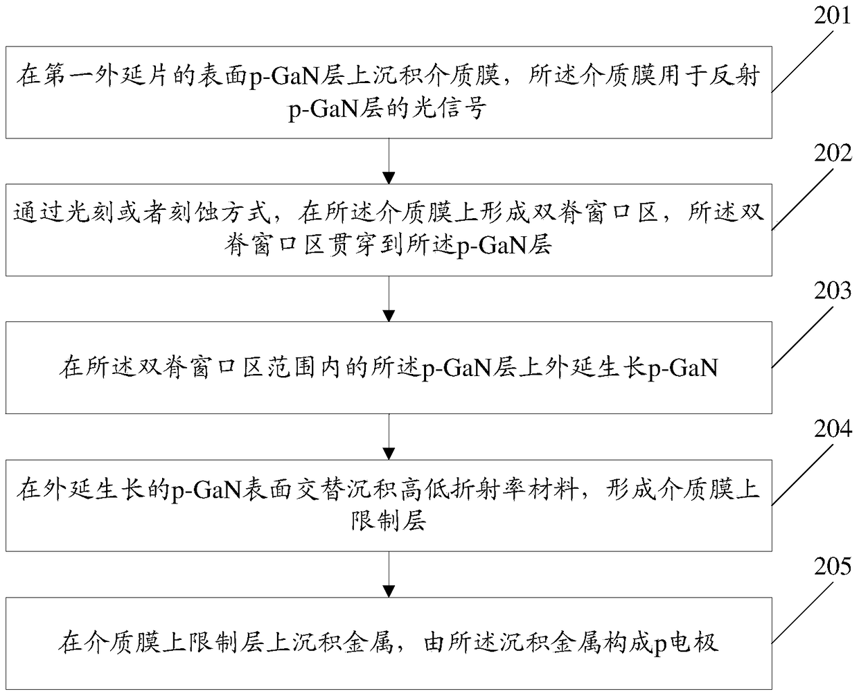
[0046] Such asfigure 1 Shown is a GaN-based laser preparation method provided by the present invention, and the preparation method includes the following steps:

[0047] In step 201, a dielectric film is deposited on the surface p-GaN layer of the first epitaxial wafer;

[0048] In step 202, a double ridge window region is formed on the dielectric film by photolithography or etching, and the double ridge window region penetrates to the p-GaN layer;

[0049] In step 203, epitaxially grow p-GaN on the p-GaN layer within the range of the double ridge window region;

[0050] In step 204, high and low refractive index materials are alternately deposited on the surface of the epitaxially grown p-GaN to form a confinement layer on the dielectric film.

[0051] In step 205, metal is deposited on the confinement layer on the dielectric film, and the p-electrode is formed by the deposited metal.

[0052] The laser of the present invention uses a dielectric film to form the upper confi...

Embodiment 2

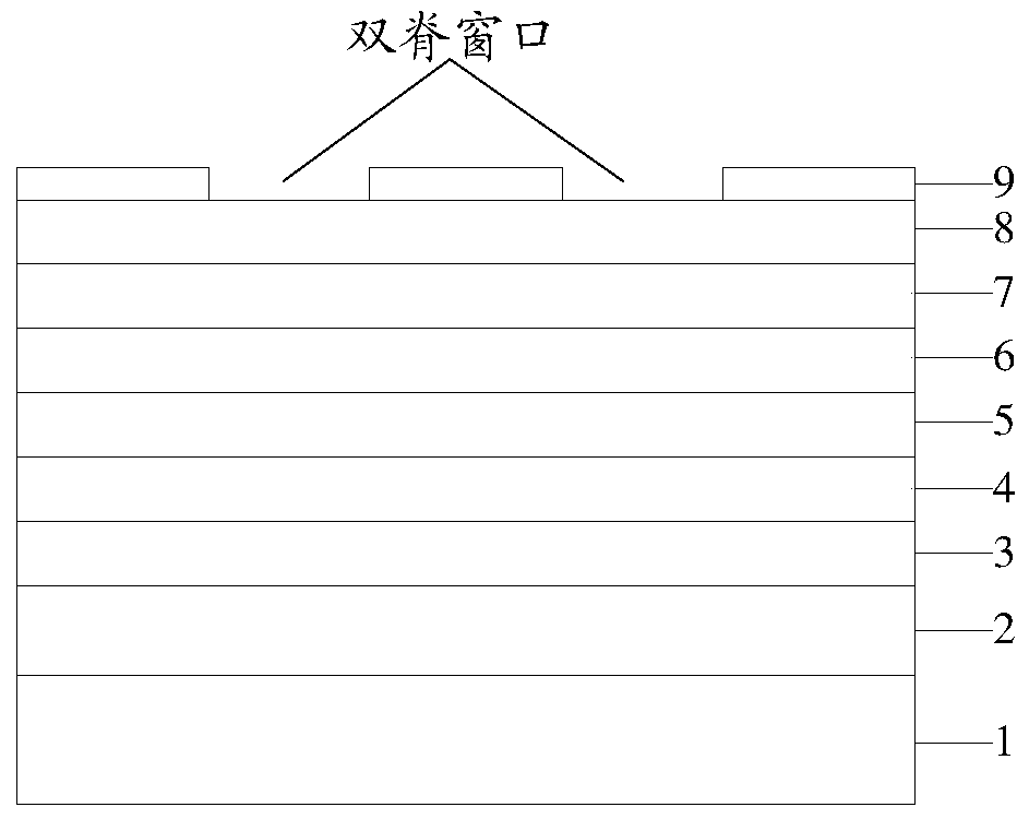
[0062] Corresponding to the method for manufacturing a GaN-based laser described in Embodiment 1, the present invention also provides a specific embodiment of the intermediate product (second epitaxial wafer) of the manufacturing process. Next, a GaN-based second epitaxial wafer is described in detail, such as Figure 4 As shown, the second epitaxial wafer includes the first epitaxial wafer 0, a dielectric film 9, a p-GaN spine 10 and a confinement layer 12 on the dielectric film, specifically:

[0063] The dielectric film is located on the p-GaN layer 8 of the first epitaxial wafer, and the dielectric film has double ridge windows (such as image 3 shown);

[0064] The p-GaN spine 10 is located in the double ridge window and is connected to the p-GaN layer 8 of the first epitaxial wafer;

[0065] The confinement layer 12 on the dielectric film is located on the p-GaN spine 10 , wherein the confinement layer on the dielectric film is made of materials with different refracti...

Embodiment 3

[0069] Corresponding to a GaN-based laser preparation method described in Embodiment 1, the present invention also provides a structure of a GaN-based laser manufactured by it, such as Figure 5 As shown, the laser includes a first epitaxial wafer 0, a dielectric film 9, a p-GaN spine 10, a confinement layer 12 on the dielectric film, a P electrode 11 and an N electrode (not shown in the figure), specifically:

[0070] The dielectric film 9 is located on the p-GaN layer 8 of the first epitaxial wafer 0, and the dielectric film 9 has a double ridge window;

[0071] The p-GaN spine 10 is located in the double ridge window and is connected to the p-GaN layer 8 of the first epitaxial wafer 0;

[0072] The confinement layer 12 on the dielectric film is located on the p-GaN spine 10, wherein the confinement layer 12 on the dielectric film is made of materials with different refractive indices;

[0073] The P-electrode 11 is located on the dielectric film 9, or on the dielectric fil...


PUM


Abstract

The invention is applicable to the field of a semiconductor photoelectric technology, and provides a preparation method and a structure for a GaN-based laser. The preparation method comprises the steps of depositing a dielectric film on a p-GaN layer on the surface of a first epitaxial layer; forming a dual-ridge window region in the dielectric film through a photoetching manner or an etching manner, wherein the dual-ridge window region penetrates to the p-GaN layer; performing p-GaN epitaxial growth on the p-GaN layer within the scope of the dual-ridge window region; alternatively depositing materials with high refractive index and low refractive index on the epitaxial growth p-GaN surface to form an upper limiting layer of the dielectric film; and depositing metal on the upper limiting layer of the dielectric film, wherein a p electrode is formed by the deposited metal. The upper limiting layer of the laser is formed by the dielectric film, so that the limiting factors of the laser can be effectively increased, and the internal loss is lowered; and in addition, the current is injected through the p-GaN, so that the laser resistance can be effectively reduced, the working voltage of the laser can be lowered, and the performance of the laser can be improved.

Description

technical field [0001] The invention belongs to the technical field of semiconductor optoelectronics, and in particular relates to a preparation method and structure of a GaN-based laser. Background technique [0002] III-V nitride semiconductors are called third-generation semiconductor materials, which have the advantages of large band gap, good chemical stability, and strong radiation resistance; their band gap covers the entire visible light range, so they can be used to make semiconductor light-emitting Devices such as light-emitting diodes, lasers, and superradiant tubes. Lasers and superradiant tubes based on III-V nitride semiconductors have the advantages of simple fabrication, small size, light weight, long life, and high efficiency, and have been widely used in the fields of optical communication, optical pumping, optical storage, and laser display. . [0003] Usually GaN-based lasers have a large series resistance and a high operating voltage, which is much hig...

Claims


Application Information

Patent Timeline
Patent Type & Authority Patents(China)
IPC IPC(8): H01S5/343H01S5/22
CPCH01S5/2209H01S5/34333
Inventor 李亮刘应军汤宝王任凡
Owner WUHAN TELECOMM DEVICES
Why Eureka
Try Eureka