Design method and system for a design for manufacturability simulator

A design method and manufacturing technology, applied in design optimization/simulation, CAD circuit design, instruments, etc., can solve problems such as ensuring calculation efficiency, and achieve the effect of simple calculation process

Active Publication Date: 2018-08-10
INST OF MICROELECTRONICS CHINESE ACAD OF SCI
View PDF5 Cites 0 Cited by
  • Summary
  • Abstract
  • Description
  • Claims
  • Application Information

AI Technical Summary

Problems solved by technology

[0005] The invention discloses a manufacturability design simulator design method to solve the technical problem that the existing manufacturability simulation device design method cannot ensure the calculation efficiency while realizing high-precision simulation, so as to obtain both calculation efficiency and precision. Meet the real-world needs of DFM simulator design

Method used


Image

  • Design method and system for a design for manufacturability simulator
  • Design method and system for a design for manufacturability simulator
  • Design method and system for a design for manufacturability simulator

Examples


Embodiment Construction

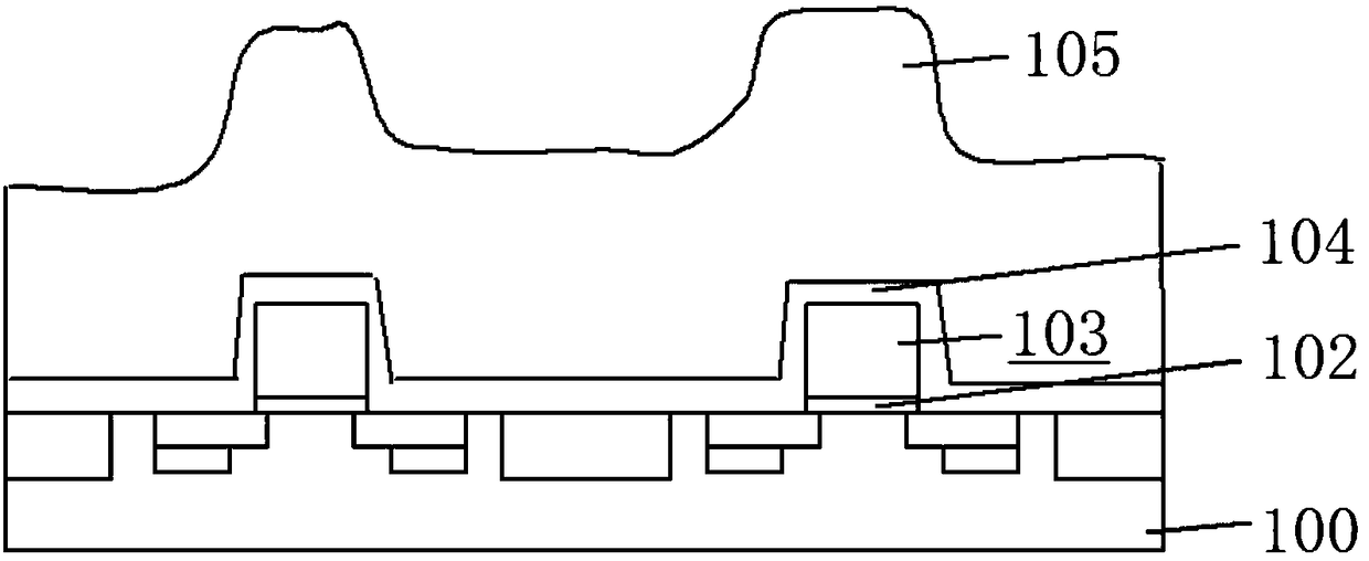
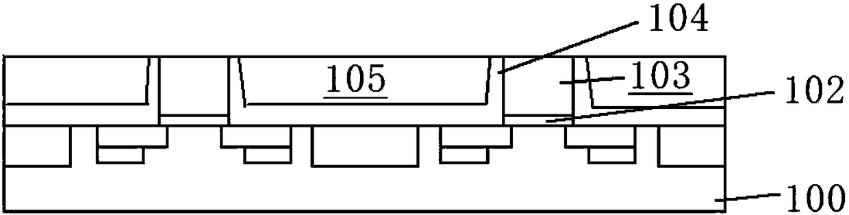
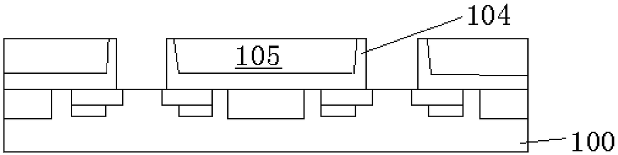
[0055] Embodiments of the present invention are described in detail below, examples of which are shown in the drawings, wherein the same or similar reference numerals designate the same or similar elements or elements having the same or similar functions throughout. The embodiments described below by referring to the figures are exemplary only for explaining the present invention and should not be construed as limiting the present invention.

[0056] Secondly, the present invention is described in detail in combination with schematic diagrams. When describing the embodiments of the present invention in detail, for the convenience of explanation, the cross-sectional view showing the device structure will not be partially enlarged according to the general scale, and the schematic diagram is only an example, and it should not be limited here. The protection scope of the present invention. In addition, the three-dimensional space dimensions of length, width and depth should be inc...


PUM


Abstract

The invention discloses a method and system for designing a design-for-manufacturability (DFM) simulator. The method comprises the steps: receiving an integrated circuit design layout, and partitioning the integrated circuit design layout into simulation grids; computing the contact pressure of each simulation grid according to the integrated circuit design layout and chemical mechanical planarization (CMP) process data; simulating the morphology of each simulation grid, subjected to a simulation execution CMP process, according to the contact pressure of each simulation grid; optimizing the integrated circuit design layout according to the morphology of each simulation grid subjected to the execution CMP process. According to the method, the computing efficiency can be guaranteed while high-accuracy simulation is achieved, so that both the computing efficiency and accuracy can meet the practical needs of DFM simulator design.

Description

technical field [0001] The invention relates to the field of semiconductor manufacturing, in particular to a design method and system for a manufacturability design simulator. Background technique [0002] With the development of the semiconductor industry, the design for manufacturability (DFM) process solution has become a frontier research hotspot in the design of integrated circuit chips. This solution provides a communication platform covering design and manufacturing information, enabling designers to advance Predict the impact of the design scheme in the process manufacturing stage, so as to realize design optimization and further reduce the reduction of chip yield caused by design defects. At the node of 32nm and below, DFM technology has become an important bridge for collaborative optimization of design and process. [0003] Chemical Mechanical Planarization (CMP), as a global planarization technology supporting DFM reference process optimization, plays a key role...

Claims


Application Information

Patent Timeline
Patent Type & Authority Patents(China)
IPC IPC(8): G06F17/50
CPCG06F30/20G06F30/39
Inventor 徐勤志陈岚
Owner INST OF MICROELECTRONICS CHINESE ACAD OF SCI
Why Eureka
Try Eureka