Annular cutting process method of Taiko thinning process

A process method and process technology, applied in the field of ring cutting process of Taiko thinning process, can solve the problems of uneven torque, film sandwich, difficult to control, etc., and achieve the effect of reducing the fragment rate and the separation process is stable.

Active Publication Date: 2016-03-23
SHANGHAI HUAHONG GRACE SEMICON MFG CORP
View PDF4 Cites 16 Cited by
  • Summary
  • Abstract
  • Description
  • Claims
  • Application Information

AI Technical Summary

Problems solved by technology

[0007] In the final ring cutting process, the UV film and the support ring 2 on the edge of the wafer 1 are more viscous, so that a larger force is required in the one-time cutting process and the torque will be uneven during the cutting process, and it is not easy to continue a large torque. Controlled and easy to cause the problem of clamping film and debris during the process of taking the ring

Method used


Image

  • Annular cutting process method of Taiko thinning process
  • Annular cutting process method of Taiko thinning process
  • Annular cutting process method of Taiko thinning process

Examples


Embodiment Construction

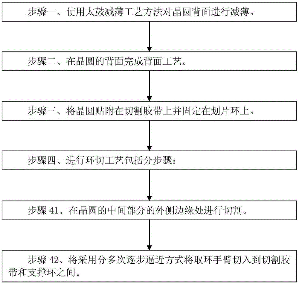
[0025] Such as figure 2 Shown is the flow chart of the method of the embodiment of the present invention; Figure 3A to Figure 3C Shown is a schematic diagram of the ring cutting process of the method of the embodiment of the present invention. The circumcision process method of the Taiko drum thinning process in the embodiment of the present invention comprises the following steps:

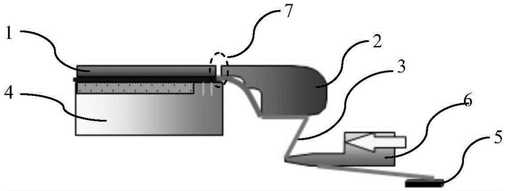
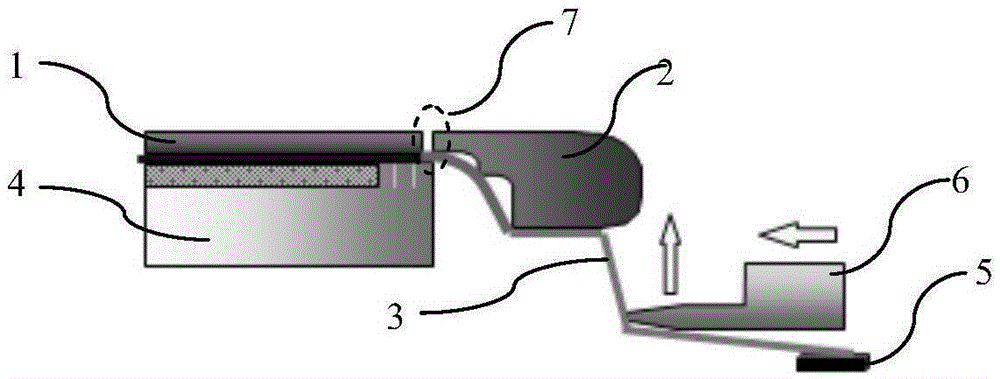
[0026] Step 1. Thinning the back of the wafer 1 using the Taiko thinning process, the middle part of the wafer 1 is thinned to the required thickness, and the edge part of the wafer 1 is not thinned to form a support ring 2.

[0027] Step 2, completing the backside process on the backside of the thinned wafer 1 .

[0028] Step 3: Attach the wafer 1 that has completed the backside process on the dicing tape 3 and fix it on the dicing ring 5 . Preferably, the dicing tape 3 is an ultraviolet irradiation tape or a heat sensitive tape.

[0029] Wherein, the surface of the wafer 1 is placed on th...


PUM


Abstract

The invention discloses an annular cutting process method of a Taiko thinning process. The annular cutting process method comprises the following steps of thinning the back surface of a wafer by the Taiko thinning process method; completing a back surface process on the back surface of the wafer; and attaching the wafer onto a cutting adhesive tape and fixing the wafer on a scribing ring. The annular cutting process comprises the following steps of cutting an edge of an outer side at the middle part of the wafer; and cutting a ring taking arm to be between the cutting adhesive tape and a support ring by a successive approximation mode in multiple times. By the annular cutting process, the debris rate in the annular cutting step can be reduced.

Description

technical field [0001] The invention relates to a manufacturing process method of a semiconductor integrated circuit, in particular to a circumcutting process method of a Taiko thinning process. Background technique [0002] The Taiko thinning process is an ultra-thin thinning process developed by DISCO Corporation of Japan. The Taiko thinning process does not thin the entire plane of the wafer, that is, the silicon wafer, but only thins the middle part of the wafer. , the edge portion of the wafer is not ground and thinned, the width of the edge portion without thinning is about 2 mm to 5 mm, and the support ring is formed by the edge portion without thinning. [0003] Generally, when the silicon wafer is thin to a certain extent and has a large area, its mechanical strength will be greatly reduced. Taking an 8-inch silicon wafer as an example, when the thickness of the silicon wafer is less than 200 microns, the silicon wafer will be curled, so it cannot continue to be tra...

Claims


Application Information

Patent Timeline
Patent Type & Authority Applications(China)
IPC IPC(8): H01L21/02H01L21/304
CPCH01L21/02H01L21/304
Inventor 郁新举
Owner SHANGHAI HUAHONG GRACE SEMICON MFG CORP
Why Eureka
Try Eureka