
A high-power laser bar chip sintering fixture

A technology of high-power lasers and fixtures, applied in lasers, laser components, semiconductor lasers, etc., can solve the problem of double beam quality reduction, affecting semiconductor laser beam propagation, focusing, shaping, and increasing off-axis images of fast-axis collimator mirrors Poor and other problems, to achieve the effect of correcting bending, improving production efficiency, and ensuring beam quality

Active Publication Date: 2018-05-25
THE 13TH RES INST OF CHINA ELECTRONICS TECH GRP CORP
View PDF5 Cites 0 Cited by
  • Summary
  • Abstract
  • Description
  • Claims
  • Application Information

AI Technical Summary

Problems solved by technology

The smile effect increases the off-axis aberration of the fast-axis collimator. Usually, the smile effect of 5 μm can cause a 2-fold reduction in beam quality, which seriously affects the propagation, focusing, and shaping of the semiconductor laser beam. Therefore, the smile effect gives the array semiconductor laser beam coupling and beam shaping pose a huge challenge, which has become the most important obstacle to limit the expansion of semiconductor laser arrays

Method used


Image

  • A high-power laser bar chip sintering fixture
  • A high-power laser bar chip sintering fixture
  • A high-power laser bar chip sintering fixture

Examples


Embodiment

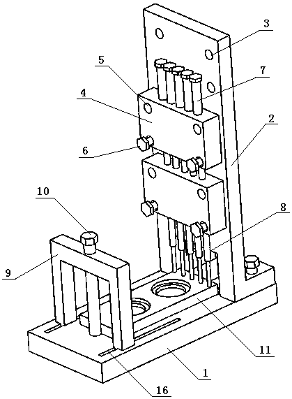
[0028] The present invention needs to apply according to the actual bending situation: the pressure gradually decreases from the middle to both ends of the chip; it includes 5 spring probes, and the pressure of each spring probe can apply different pressures by changing different lengths. Among them, the pressure of the middle spring probe is 2N, the pressure of the spring probe next to the middle spring probe is 1N, and the pressure of the edge spring probe is 0.5N. Through different pressures of spring probes, different pressures are applied to different parts of the chip to achieve smile optimization, which reduces the bending value of 3-4um produced by the previous smile effect to 1.5um, improves the beam quality of the chip, and greatly improves the semiconductor laser beam Spread, focus, shape.


PUM


Abstract

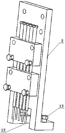
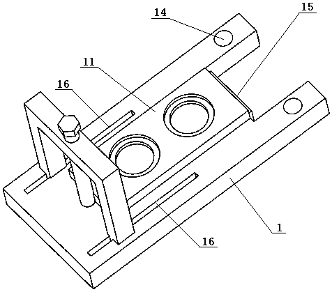
The invention discloses a high-power laser strip-type chip sintering clamp, and relates to the field of a semiconductor photoelectric technology. The high-power laser strip-type chip sintering clamp comprises a clamp base, a positioning plate, a probe positioning apparatus and spring probes, wherein a check block for limiting heat sink is arranged at one end of the clamp base while a positioning mechanism for positioning the heat sink is arranged at the other end of the clamp base; the positioning plate is perpendicularly mounted at the end of the clamp base through a fastener, wherein the heat sink check block is fixed at the end of the clamp base; a plurality of uniformly distributed through holes are formed in the probe positioning apparatus, wherein the through holes are adaptive with the spring probes; the spring probes are inserted in the positioning through holes respectively; the bottom ends of the spring probes are positioned above the heat sink and used for compressing to-be-sintered chips; and threads are further formed in the top parts of the positioning through holes, and the threads are matched with adjustable bolts for adjusting the magnitude of torsion of the spring probes. The clamp can apply different pressures on different parts of the high-power laser chip by the spring probes on the positioning plate so as to balance the stresses of the chip, correct smile bending degree and improve the optical beam quality of the chip.

Description

technical field [0001] The invention relates to the technical field of semiconductor optoelectronics. Background technique [0002] High-power semiconductor lasers (LD) and their pumped solid-state lasers have the advantages of small size, light weight, high photoelectric conversion efficiency, stable performance, high reliability and long life, and have become the most promising products in the optoelectronic industry. Widely used in industrial, military, medical and direct material processing and other fields. As the demand for pumping of high-power lasers increases, it is necessary to superimpose the number of single lasers to increase the total power of the pumping source. The more the number of single lasers, the higher the requirements for the beam quality of high-power semiconductor lasers. [0003] When the high-power semiconductor laser array is working, each light-emitting unit is not in a straight line, which causes the overall light-emitting of the LDA to bend,...

Claims


Application Information

Patent Timeline
Patent Type & Authority Patents(China)
IPC IPC(8): H01S5/022H01S5/024
CPCH01S5/02407H01S5/02325
Inventor 房玉锁徐会武沈牧任永学王伟
Owner THE 13TH RES INST OF CHINA ELECTRONICS TECH GRP CORP
Learn More