Linewidth compensation method for manufacturing printed circuit board
A technology for making printed circuit boards and circuits, which is applied in the fields of printed circuit manufacturing, printed circuits, electrical components, etc. It can solve problems such as excessive circuit burrs, poor quality of circuit boards, and scrapping, and achieve the effect of improving product quality
- Summary
- Abstract
- Description
- Claims
- Application Information
AI Technical Summary
Problems solved by technology
Method used
Image
Examples
Embodiment Construction
[0016] The present invention will be further described below in conjunction with the accompanying drawings and embodiments.
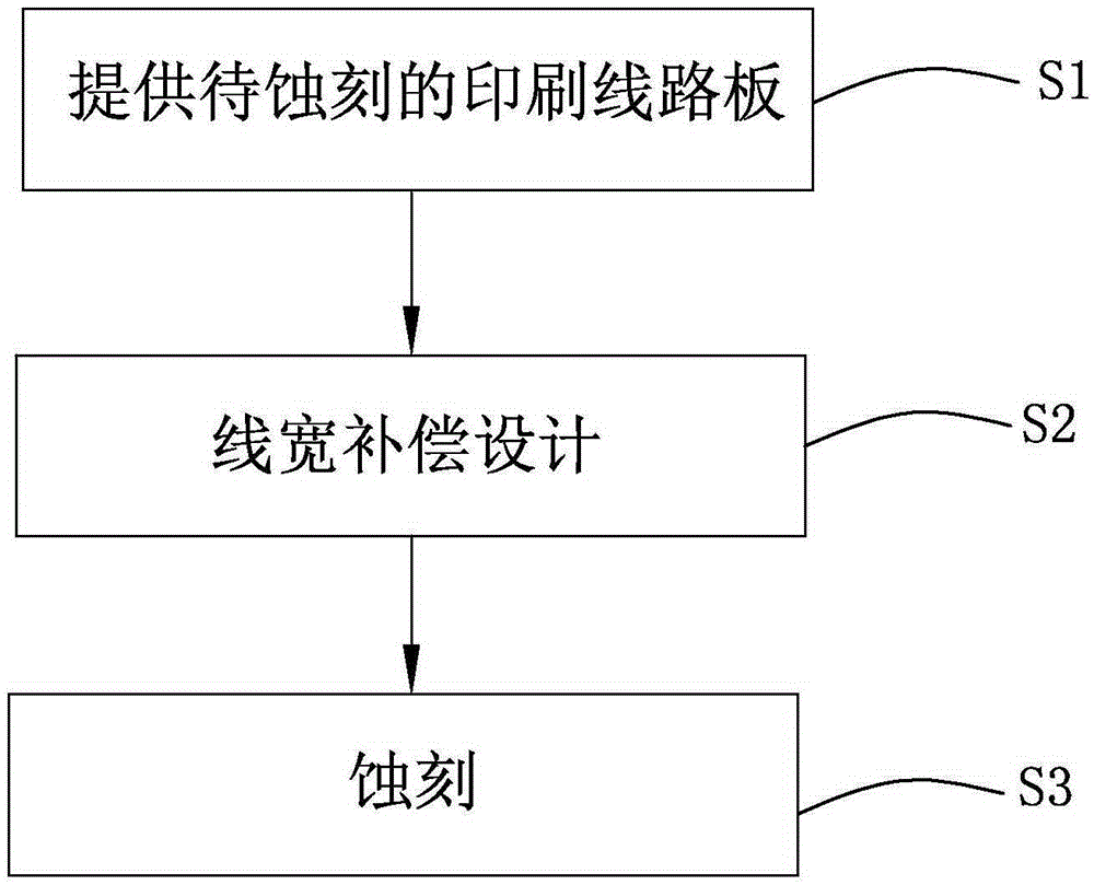
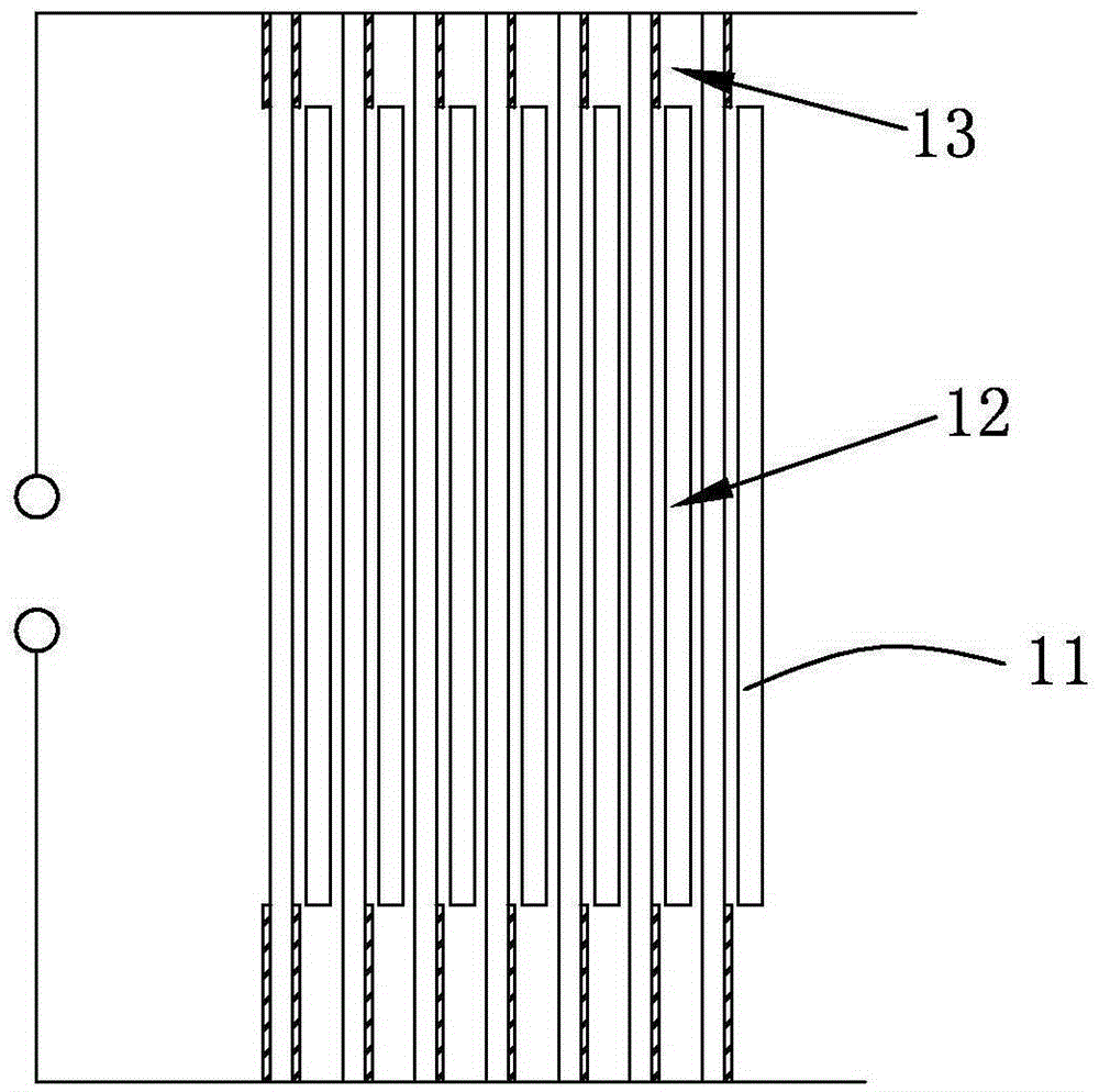
[0017] Please refer to figure 1 with figure 2 ,in, figure 1 A flow chart of the line width compensation method made for the printed circuit board of the present invention, figure 2 It is a schematic diagram of circuit distribution in the printed circuit board of the present invention. The line width compensation method for making the printed circuit board includes:
[0018] Step S1, providing a printed circuit board to be etched, which includes a developed dense circuit area 12 and a sparse circuit area 13;
[0019] In step S1, a printed circuit board to be etched with a preset bottom copper thickness is provided. Specifically, the thickness of the bottom copper is 23um, the dense line area 12 is the area where the distance between adjacent copper foils 11 is less than or equal to 0.075mm, and the sparse line area 13 is the area where the distanc...
PUM
 Abstract
Description
Claims
Application Information

